Thin layer metal chemical vapor deposition

a thin layer metal and chemical vapor technology, applied in the direction of chemically reactive gases, crystal growth process, polycrystalline material growth, etc., can solve the problems of poor nucleation of copper at the barrier layer, affecting the insulating electrical properties, and not always providing conformal step coverag

Inactive Publication Date: 2005-02-01
NOVELLUS SYSTEMS
View PDF3 Cites 115 Cited by
  • Summary
  • Abstract
  • Description
  • Claims
  • Application Information

AI Technical Summary

Benefits of technology

In one important application, the method deposits a seed layer suitable for subsequent electro-deposition of a bulk layer of metal on the partially fabricated integrated circuit. Electro-de

Problems solved by technology

While copper has a greater conductivity than aluminum, it has not been used because of certain challenges it presents, including the fact that it readily diffuses into silicon oxide and degrades insulating electrical properties even at very low concentrations.
PVD has traditionally been used to form the seed layer, but does not always provide conformal step coverage, particularly with surface features having high aspect ratios (greater than about 5:1).
However, poor nucleation of the copper at the barrier layer is a common problem with CVD, as is agglomeration.
These problems result, in part, because copper itself does not adhere well to most materials.
Further, the relatively high t

Method used


Image

  • Thin layer metal chemical vapor deposition
  • Thin layer metal chemical vapor deposition
  • Thin layer metal chemical vapor deposition

Examples


Embodiment Construction

Introduction

In the following detailed description of the present invention, numerous specific embodiments are set forth in order to provide a thorough understanding of the invention. However, as will be apparent to those skilled in the art, the present invention may be practiced without these specific details or by using alternate elements or processes. In other instances well-known processes, procedures and components have not been described in detail so as not to unnecessarily obscure aspects of the present invention.

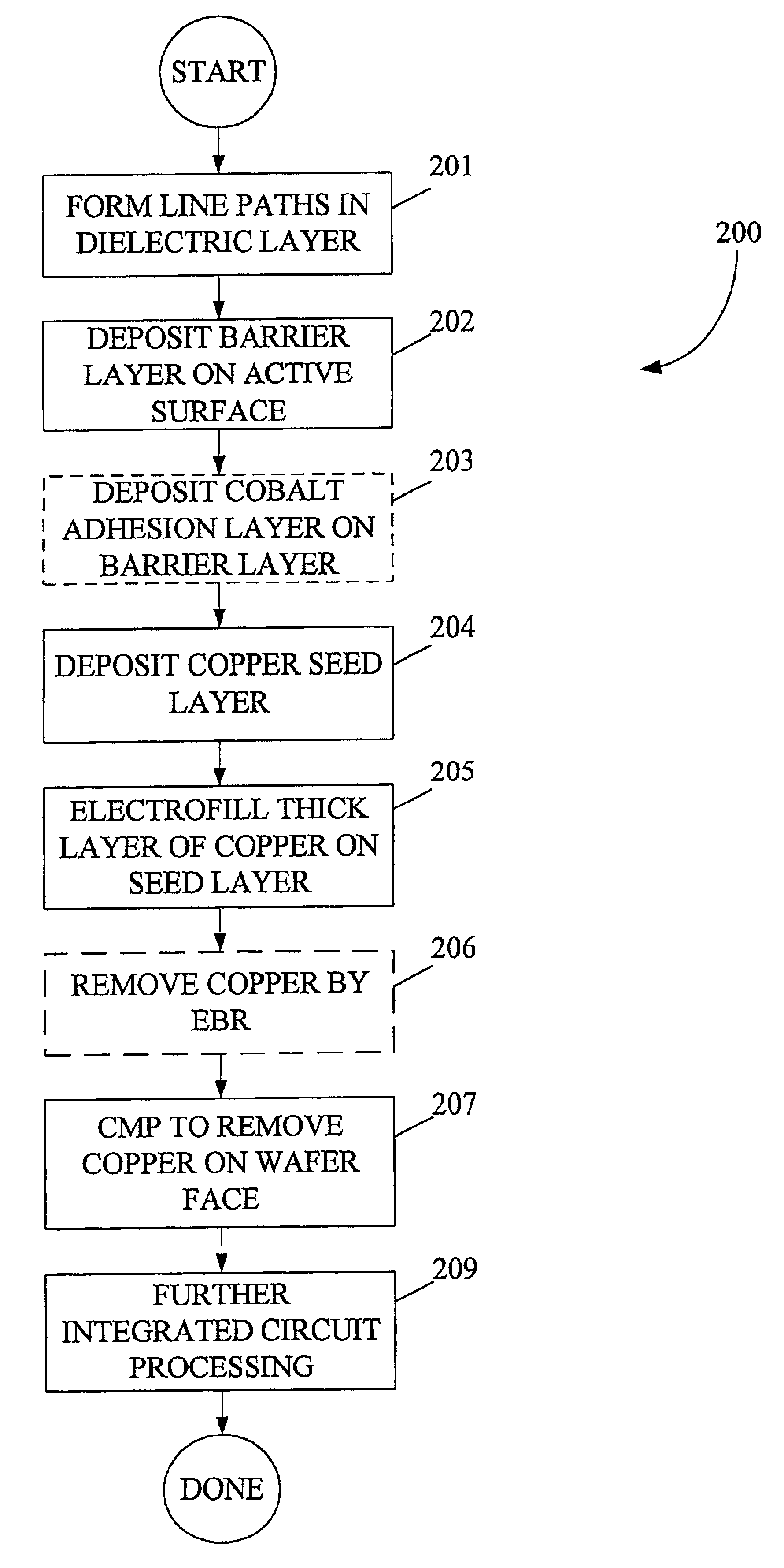
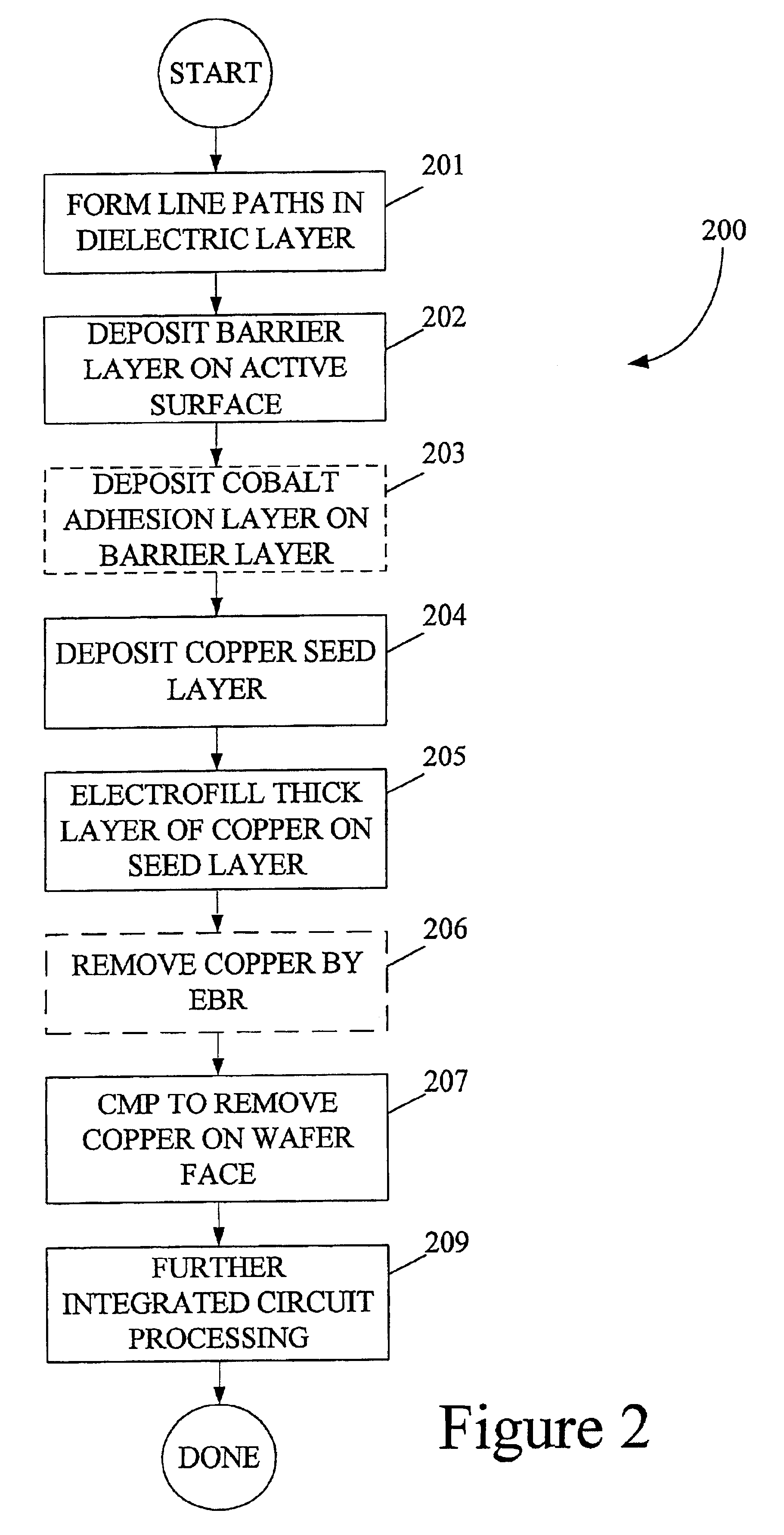
As used herein, the term “metal layer” refers to a thin conformal or reasonably conformal film of metal residing on a substrate surface. As indicated, the methods of this invention produce “metal layers.” In many embodiments of this invention, the metal layer is formed via one or more cycles of (i) precursor deposition, (ii) precursor oxidation, and (iii) oxide reduction. During each cycle, the deposited metal layer is very thin, on the order of 1 to 50 atomic layers....


PUM

PropertyMeasurementUnit
Lengthaaaaaaaaaa
Diffusion barrieraaaaaaaaaa
Electrical conductoraaaaaaaaaa

Abstract

A CVD method deposits conformal metal layers on small features of a substrate surface. The method includes three principal operations: depositing a thin conformal layer of precursor over some or all of the substrate surface; oxidizing the precursor to convert it to a conformal layer of metal oxide; and reducing some or all of the metal oxide to convert it to a conformal layer of the metal itself. The conformal layer of precursor may form a “monolayer” on the substrate surface. Examples of metals for deposition include copper, cobalt, ruthenium, indium, and rhodium.

Description

FIELD OF THE INVENTIONThis invention pertains to systems and methods and apparatus for metal deposition. More specifically, the invention pertains to methods that deposit a thin layer of metal precursor, then oxidize the precursor to form an oxide, and finally reduce the oxide to the metal itself.BACKGROUND OF THE INVENTIONIntegrated circuit (IC) manufacturers have traditionally used aluminum and aluminum alloys, among other metals, as the conductive metal for integrated circuits. While copper has a greater conductivity than aluminum, it has not been used because of certain challenges it presents, including the fact that it readily diffuses into silicon oxide and degrades insulating electrical properties even at very low concentrations. Recently, however, IC manufacturers have nevertheless turned to copper. Most notable among the IC metalization processes that use copper is Damascene processing.Damascene processing is a method for forming metal lines on integrated circuits. It invol...

Claims


Application Information

Patent Timeline
IPC IPC(8): C23C16/56C23C16/18C30B25/02C23C16/44C23C16/455
CPCC23C16/18C23C16/45525C23C16/56C30B25/02C30B29/02H01L21/28562H01L21/76873
Inventor FAIR, JAMES A.
Owner NOVELLUS SYSTEMS
Why Eureka
Try Eureka