Method of forming an isolation layer in a semiconductor devices

Inactive Publication Date: 2005-02-01
SK HYNIX INC
View PDF3 Cites 27 Cited by
  • Summary
  • Abstract
  • Description
  • Claims
  • Application Information

AI Technical Summary

Benefits of technology

Accordingly, a method for forming an isolation layer in a semiconductor device, is disclosed which is capable of simultaneously preventing a concentration of the electric field and formation of a moat. The disclosed method forms the isolating film by forming a V-type trench at the isolation region, implanting ions capable of accelerating oxidization action i

Problems solved by technology

There is a problem in that the top corner of the trench may not be formed locally within the wa

Method used


Image

  • Method of forming an isolation layer in a semiconductor devices
  • Method of forming an isolation layer in a semiconductor devices
  • Method of forming an isolation layer in a semiconductor devices

Examples


Embodiment Construction

Reference will now be made in detail to the preferred embodiments, examples of which are illustrated in the accompanying drawings, in which like reference numerals are used to identify the same or similar parts.

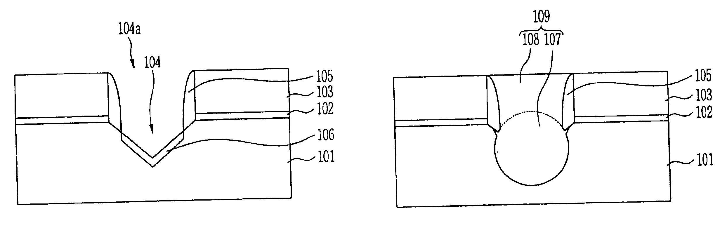
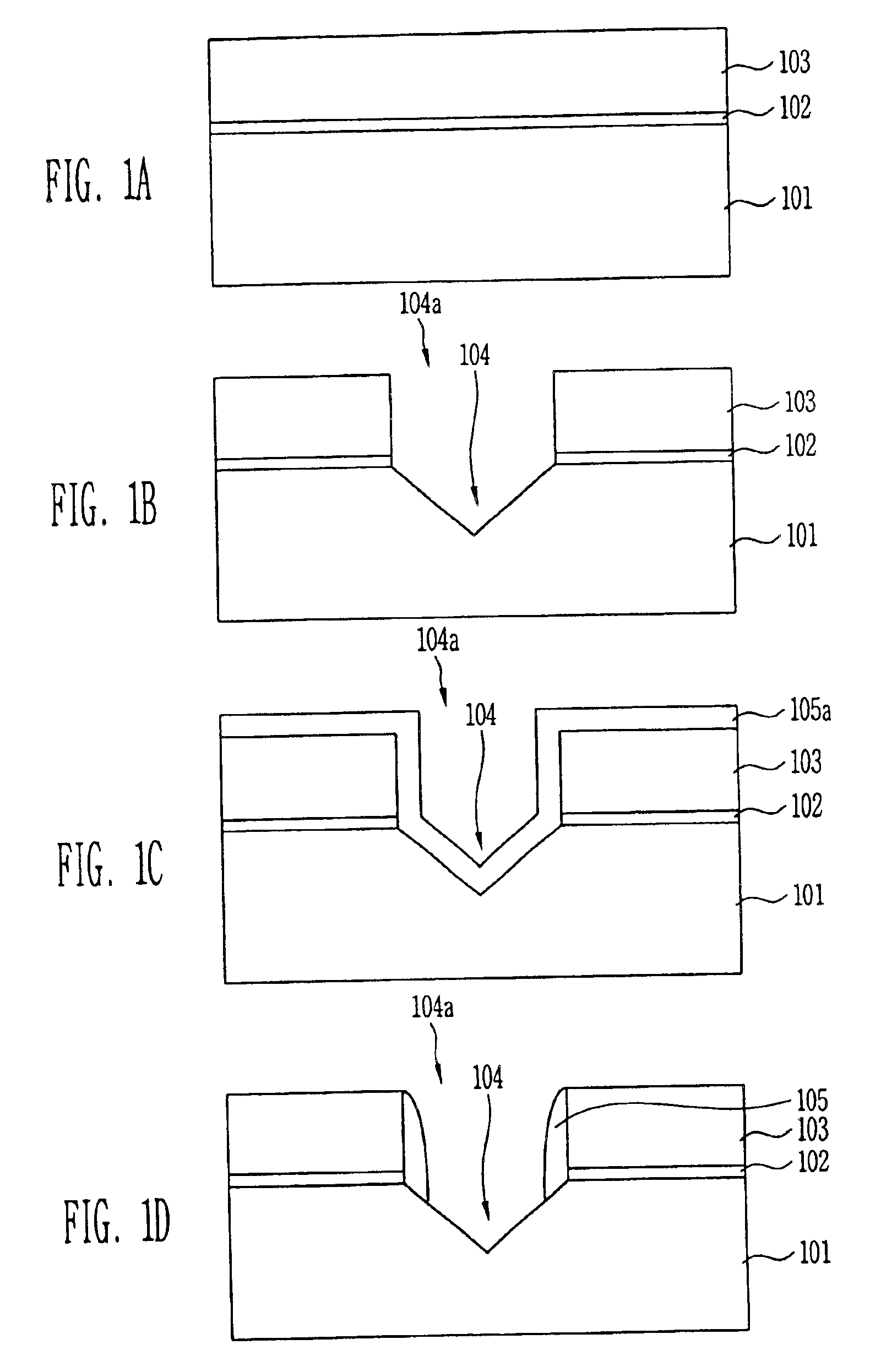
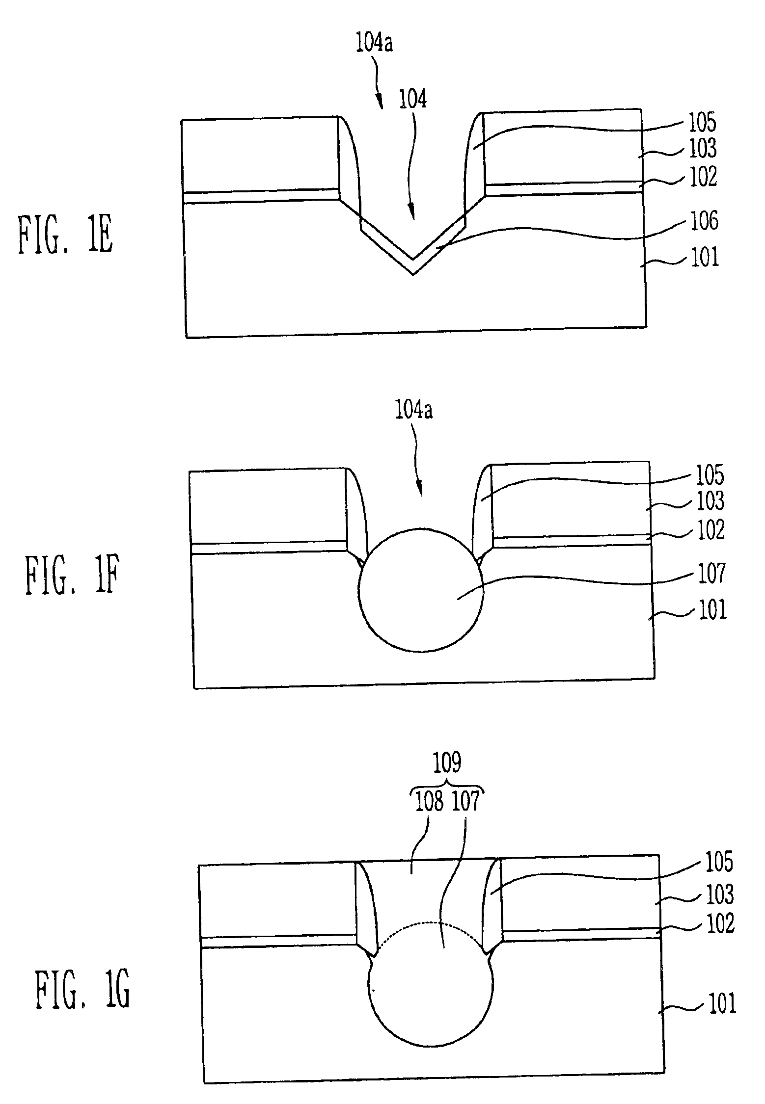
A method of forming an isolation layer in the semiconductor devices will be now described in detail by reference to FIG. 1A through FIG. 1L.

Referring now to FIG. 1A, a pad oxide film 102 and a pad nitride film 103 are sequentially formed on a semiconductor substrate 101, in order to prohibit generation of crystal defects on the entire structure and implement surface processing.

The pad oxide film 102 is formed in thickness of 50˜70 Å by means of dry oxidization mode or wet oxidization mode at a temperature of 750˜900° C. Further, the pad nitride film 103 may be formed in thickness of 700˜2000 Å by means of LP-CVD method. At this time, the thickness of the pad nitride film 103 is not limited to the above value. Instead, the thickness of the pad nitride film 103 may be determine...


PUM


Abstract

A method of forming an isolation layer in semiconductor devices is disclosed. The method includes forming the isolating film by means of a method in which a method of forming a V-type trench at the isolation region, implanting ions capable of accelerating oxidization action into the center portion of the V-type trench, implementing an oxidization process to form an insulating film consisting of an oxide film at the isolation region, and then completely burying the trench with an insulating material, using the LOCOS method, and a method of forming a trench type isolation layer, are applied together. Therefore, as the top corner of the trench is formed with an inclination, and a concentration of the electric field and a formation of a moat can be simultaneously prevented.

Description

BACKGROUNDTechnical FieldA method for forming an isolation layer in the semiconductor device is disclosed, which is capable of simultaneously preventing a concentration of an electric field on a top corner of a trench and formation of an undesirable moat.BACKGROUND OF THE RELATED ARTIn all the processes of manufacturing semiconductor devices, an isolation layer is formed in an isolation region in order to electrically isolate respective devices formed at the semiconductor substrate. In the prior art, the isolation layer is formed by LOCOS (local oxidation) process. As the degree of integration of the semiconductor device increases, however, the isolation layer has recently been formed by means of a process of etching the semiconductor substrate by a given depth to form the trench and the trench is buried with an insulating material. The isolation layer formed thus is called a trench-type isolation layer.The trench-type isolation layer is formed by forming a pad oxide film and a pad ...

Claims


Application Information

Patent Timeline
IPC IPC(8): H01L21/762H01L21/70H01L21/76H01L21/265
CPCH01L21/76205H01L21/76235H01L21/76213H01L21/76
Inventor DONG, CHA DEOK
Owner SK HYNIX INC
Why Eureka
Try Eureka