Method for manufacturing semiconductor device
a manufacturing method and semiconductor technology, applied in semiconductor devices, semiconductor/solid-state device details, electrical devices, etc., can solve the problems of over-etching, electrical connection between unexpected regions, and inability to connect holes with lower layer wiring, etc., to achieve high electric reliability and high integration
- Summary
- Abstract
- Description
- Claims
- Application Information
AI Technical Summary
Benefits of technology
Problems solved by technology
Method used
Image

Examples
first embodiment
A method for manufacturing a semiconductor device according to the present invention will now be discussed with reference to the drawings.
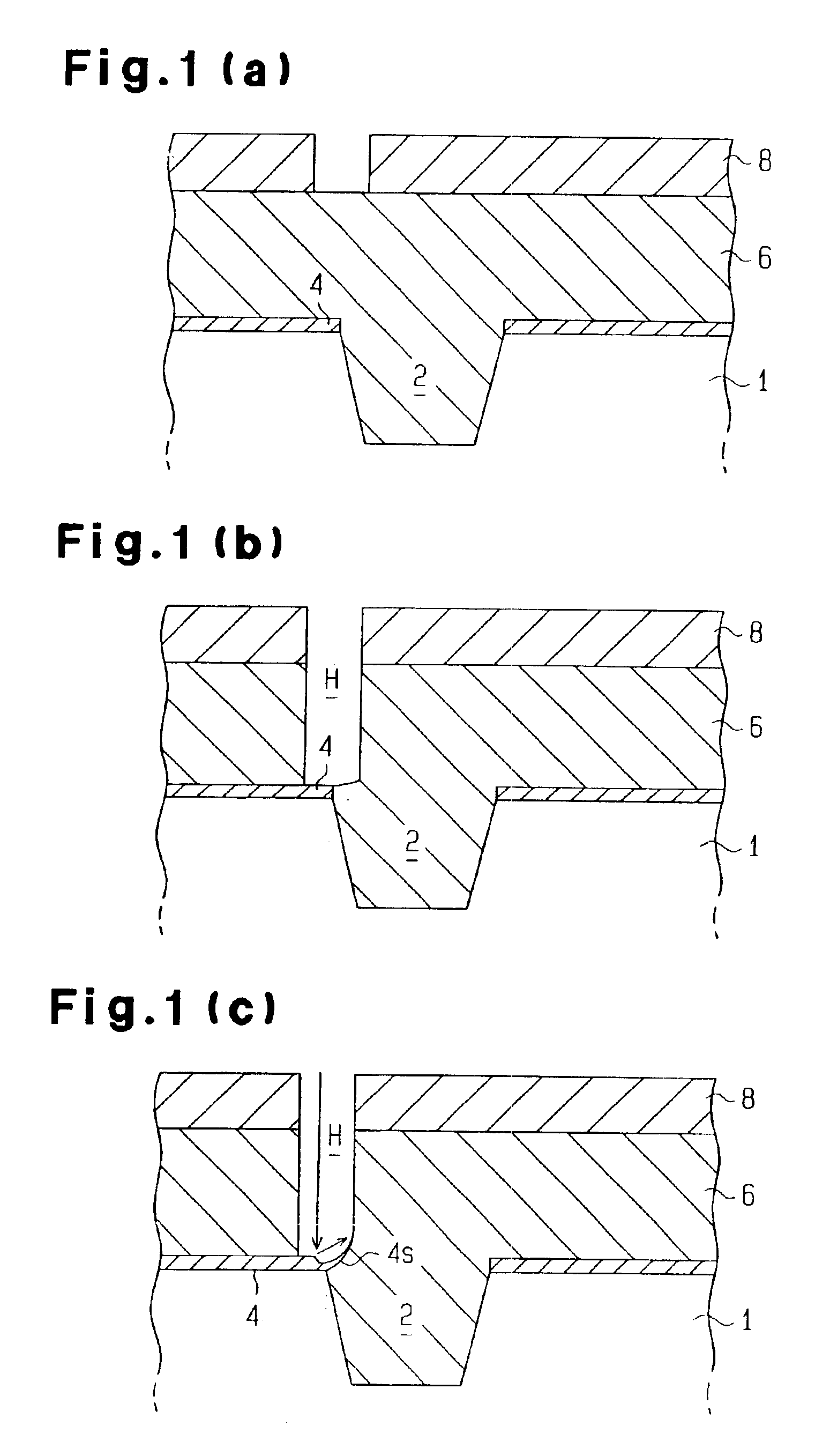
FIG. 1(a) is a partial cross-sectional view showing a semiconductor device that is undergoing manufacturing. As shown in FIG. 1(a), an element separation groove 2, a gate 4, and an interlayer insulation film 6 are sequentially formed on a semiconductor substrate 1. Then, a resist pattern 8 is applied to the interlayer insulation film 6 to form an opening in the interlayer insulation film 6 and establish contact between the gate 4 and the upper wiring layer. In the first embodiment, the gate 4 has a silicide configuration, such as Ti, Co, or Ni. Further, the interlayer insulation film 6 is formed from a silicon oxidation film.
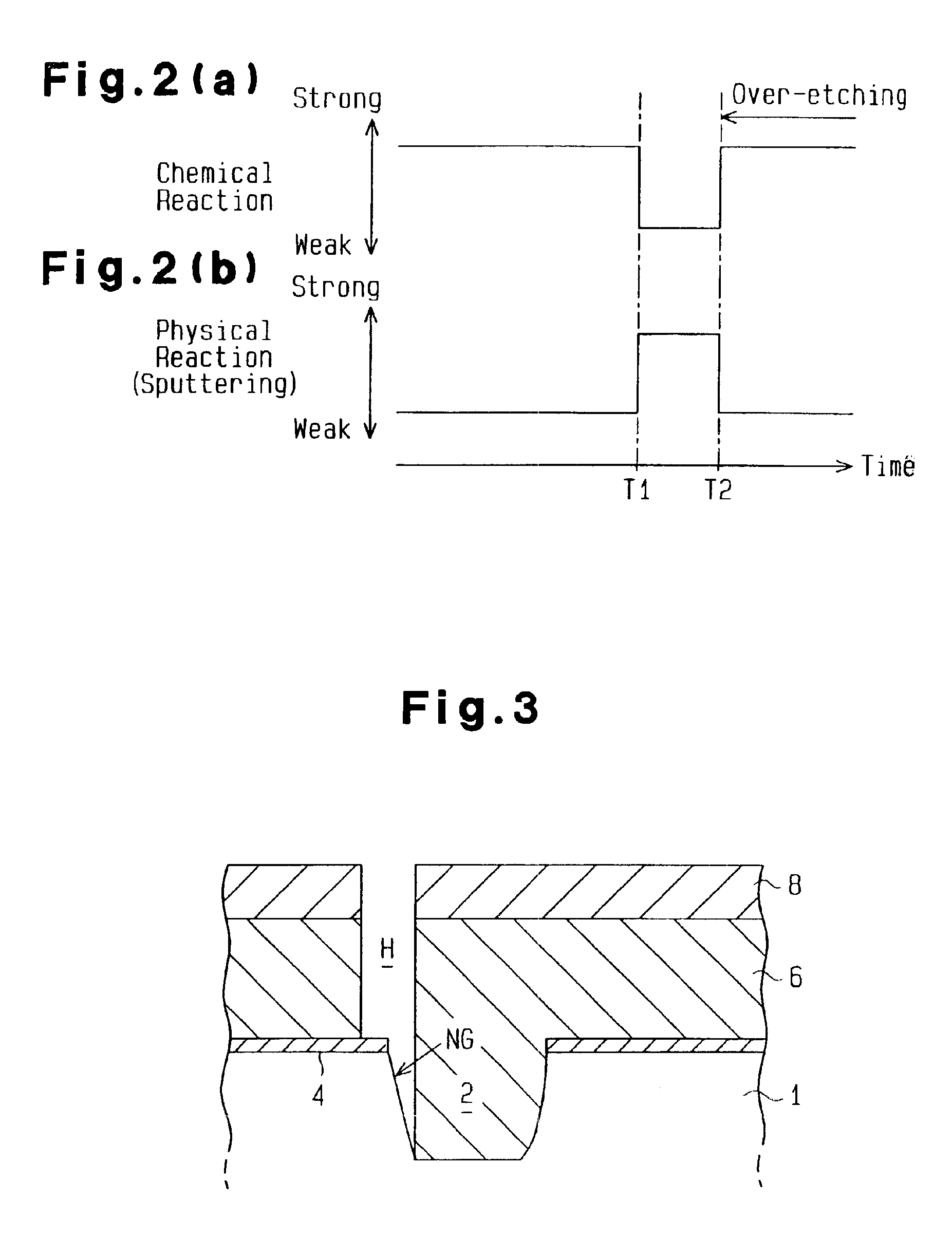
Reactive ion etching is normally performed to form an opening in the interlayer insulation film 6. Reactive ion etching is performed by using an etching gas, which is generated by ionizing active gas chemically reacting to the...
second embodiment
In the second embodiment, the electric reliability between wiring layers is guaranteed in the following manner when forming the air layer.
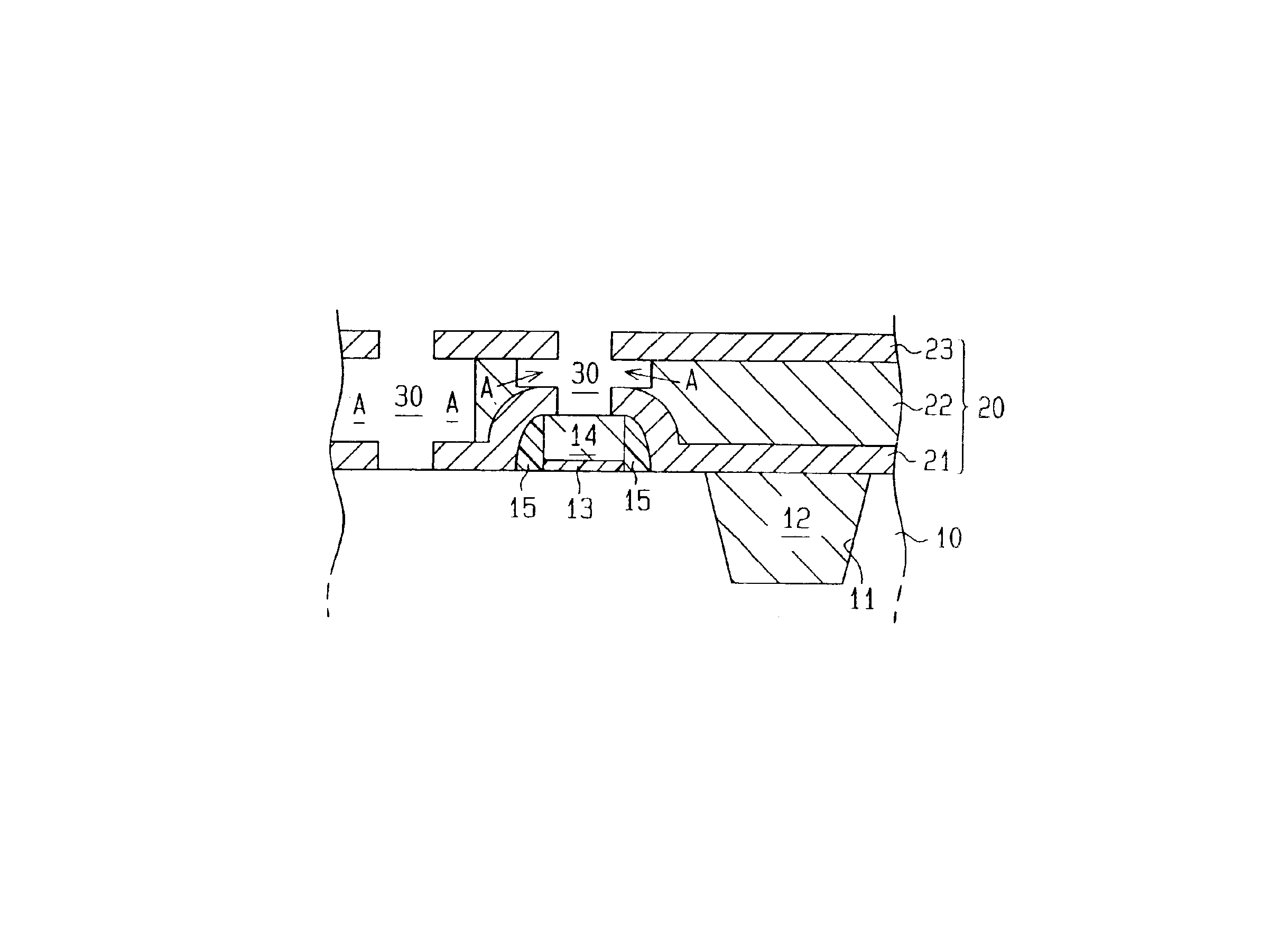
As shown in FIG. 4(a), the semiconductor device has an element separation groove 11 formed in a semiconductor substrate 10. An insulation body 12 is embedded in the element separation groove 11 to form an element separation region, which separates the semiconductor substrate 10 into element regions. Elements, such as a gate insulation film 13, a polysilicon gate 14, and spacers 15 formed about the sides of the gate insulation film 13 and the polysilicon gate 14, are formed in the element region.
An interlayer insulation film 20 covers the upper side of the semiconductor substrate 10, on which the elements are formed. The interlayer insulation film 20 includes a lower layer 21, an upper layer 23, and an intermediate layer 22, which is formed from a material differing from that of the lower layer 21 and the upper layer 23. The upper layer 23 and the ...
third embodiment
The third embodiment has the advantages described below.
A pattern insulation film having a predetermined pattern and made of a material that differs from that of the interlayer insulation film is formed in the interlayer insulation film. The pattern insulation film is selectively etched and removed to form the air layer. This improves the characteristic for controlling the shape of the air layer.
In a method for manufacturing a semiconductor device according to a fourth embodiment of the present invention, a further interlayer insulation film including air layer is formed on the interlayer insulation layer, which includes an air layer, of the second and third embodiments. Metal is charged in the air layer to form, for example, a capacitor. After the operations of the third embodiment are completed, the following operations are performed.
Formation of a pattern insulation film in an interlayer insulation film. The pattern insulation film has a predetermined pattern and is formed from a...
PUM
 Abstract
Description
Claims
Application Information
 - R&D
- Intellectual Property
- Life Sciences
- Materials
- Tech Scout
- Unparalleled Data Quality
- Higher Quality Content
- 60% Fewer Hallucinations
Browse by: Latest US Patents, China's latest patents, Technical Efficacy Thesaurus, Application Domain, Technology Topic, Popular Technical Reports.
© 2025 PatSnap. All rights reserved.Legal|Privacy policy|Modern Slavery Act Transparency Statement|Sitemap|About US| Contact US: help@patsnap.com