This helps you quickly interpret patents by identifying the three key elements:
Problems solved by technology
Method used
Benefits of technology
Benefits of technology
Since the outer leads are led out from the side surfaces of the resin sealing body and the resin sealing bodies are structurally located on and below a tab, the MCP of the above-mentioned QFP type requires both a large mounting area and a large mounting height, which is unsuitable for mounting a the mounting board built-in a current mobile device such as a cellular phone or a mobile computer. Also, with respect to the MCP of the CSP type, since the mounting area thereof is small, it is suitable for mounting onto the mounting board of a current mobile device. Thus, the CSP type is advantageous when the package is rather multifunctional and the number of external connection pins are large. However, since an insulative board (resin board or film made of epoxy, polyimide, etc.), and ball-shaped mounting external terminals made of solder and the like are used as components, the material cost is high, a special manufacturing machine is required and the number of production steps is increased. Consequently, when the number of external connection pins is small, there arises a problem such that the CSP type MCP becomes relatively expensive. Additionally, since the ball-shaped mounting external terminals are used, its height inevitably becomes increased thereby limiting the reduction in the mounting height. Furthermore, since there are restrictions in the chip size and in the arrangement of the electrode pads in stacking the LSI chips, it is difficult to use the existing LSI chips and connect respective electrode pads between the two stacked LSI chips. Therefore, a problem occurs in that the extension of leads are restricted.
The inventors of the present invention have conducted an extensive examination to effectively solve the above-mentioned problems. Thus, an object of the present invention is to provide a multi-chip type semiconductor device, which has both a very small mounting area and mounting height and can be manufactured at low cost through using the existing production line, and to provide a manufacturing method to achieve the same.
Problems solved by technology
Since the outer leads are led out from the side surfaces of the resin sealing body and the resin sealing bodies are structurally located on and below a tab, the MCP of the above-mentioned QFP type requires both a large mounting area and a large mounting height, which is unsuitable for mounting a the mounting board built-in a current mobile device such as a cellular phone or a mobile computer.
However, since an insulative board (resin board or film made of epoxy, polyimide, etc.), and ball-shaped mounting external terminals made of solder and the like are used as components, the material cost is high, a special manufacturing machine is required and the number of production steps is increased.
Consequently, when the number of external connection pins is small, there arises a problem such that the CSP type MCP becomes relatively expensive.
Additionally, since the ball-shaped mounting external terminals are used, its height inevitably becomes increased thereby limiting the reduction in the mounting height.
Furthermore, since there are restrictions in the chip size and in the arrangement of the electrode pads in stacking the LSI chips, it is difficult to use the existing LSI chips and connect respective electrode pads between the two stacked LSI chips.
Therefore, a problem occurs in that the extension of leads are restricted.
Method used
Image
Click on the blue label to locate the original text in one second.
Reading with bidirectional positioning of images and text.
Examples
first embodiment
(First Embodiment)
Description of the first embodiment will be given in conjunction with FIGS. 1 to 13.
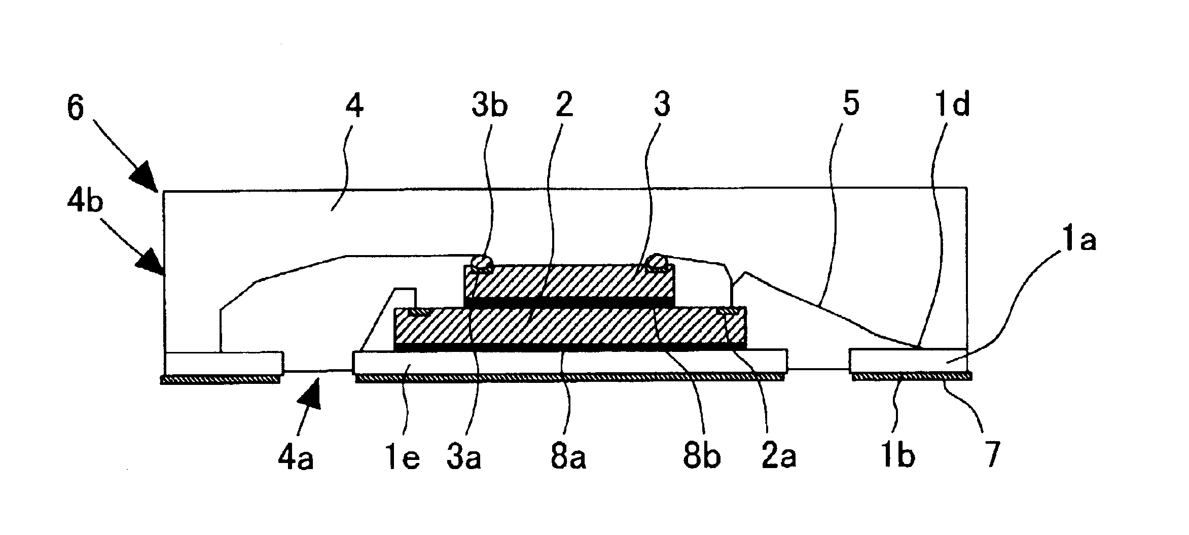
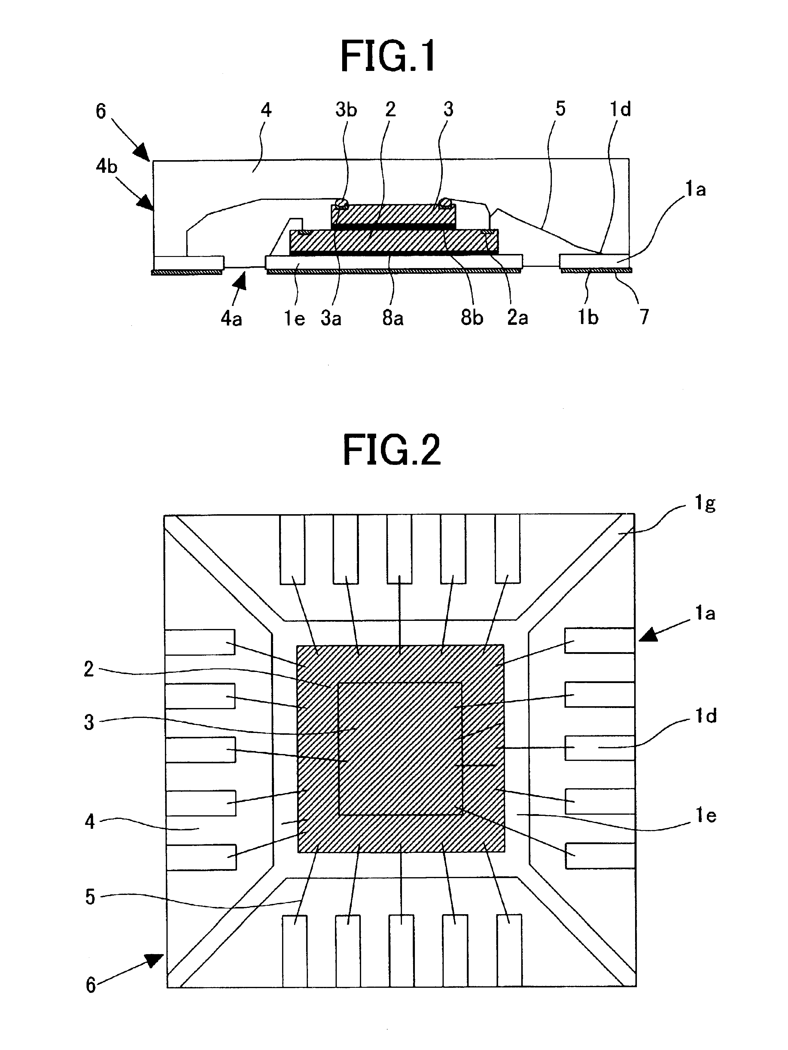
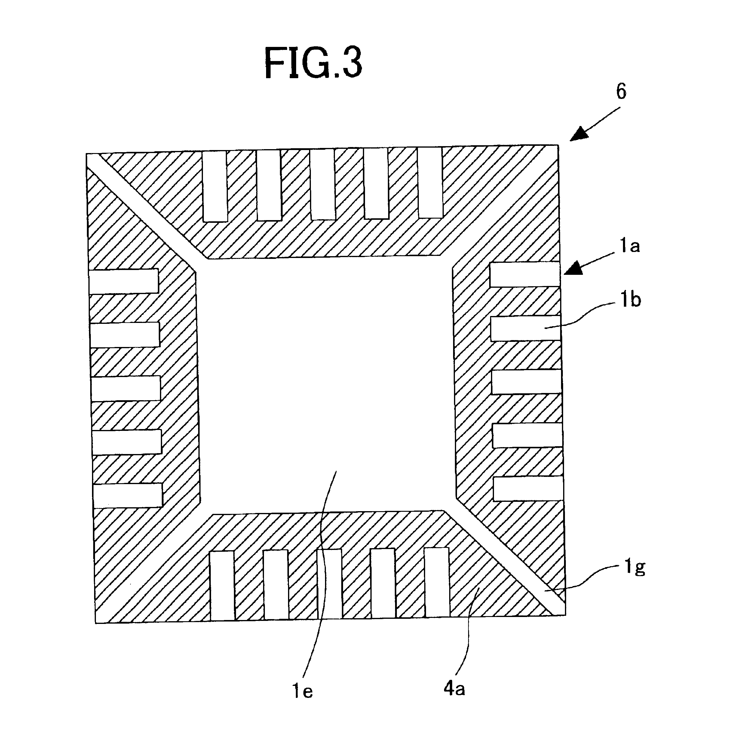
A semiconductor device shown in FIGS. 1 to 3 is a semiconductor package of a resin-sealed type and a surface-mounting type employing a lead frame. In the description of the first embodiment, the tab-exposed type semiconductor device 6 is taken as an example of this semiconductor device.
As shown in FIG. 1, in the semiconductor device 6, a first semiconductor chip 2 is adhered and supported on a second surface opposite to a first surface to be a circuit forming surface, via a conductive die bond material 8a such as silver paste or adhering film on a tab 1e (chip mounting portion). A second surface of a second semiconductor chip 3 is stacked and mounted on the first surface of the first semiconductor chip via an insulative die bond material 8b such as silicone rubber and insulative sheet, etc. Also, a plurality of electrode pads 2a and 3a of the respective semiconductor chips and a plu...
second embodiment
(Second Embodiment)
Description of the second embodiment will be given in conjunction with FIGS. 14 to 26.
The semiconductor device shown in FIGS. 14 to 16 is a semiconductor package of a resin-sealed type and a surface-mounting type employing a lead frame. In the description of a second embodiment, the semiconductor device 6 of a tab-embedded type is taken as an example of this semiconductor device.
As shown in FIG. 14, in the semiconductor device 6, a second surface of a first semiconductor chip 2, which is opposite to a first surface to be its circuit forming surface, is adhered and supported on a tab 1e (chip mounting portion) via a conductive die bond material 8a such as silver paste or adhering film. A second semiconductor chip 3 is stacked and mounted on the first surface via an insulative die bond material 8b such as silicone rubber or insulative sheet, etc. Also, a plurality of electrode pads 2a and 3a of each semiconductor chip and a plurality of leads 1a are connected by con...
third embodiment
(Third Embodiment)
FIG. 27 is a cross-sectional view showing an example of a structure of a semiconductor device according to a third embodiment of the present invention, and
FIG. 28 is a plan view showing the structure of the semiconductor device 6 shown in FIG. 27.
The semiconductor device shown in FIGS. 27 and 28 is a semiconductor package of a resin-sealed type and a surface-mounting type employing a lead frame. In the description of the third embodiment, the semiconductor device 6 is taken as an example of this semiconductor device.
As shown in FIG. 27, in the semiconductor device 6, a first surface of the first semiconductor chip 2, which is a circuit forming surface, is supported on one surface of a frame-shaped tab 1e (chip mounting portion) through, for example, silicone rubber or insulative sheet or the like. A second surface of the second semiconductor chip 3, which is opposite to a first surface thereof, is stacked and mounted on the first surface of the first semiconductor ...
PUM
Abstract
A non-lead type, stacked-type semiconductor device includes a sealing body of insulative resin, a tab, leads, each having one surface exposed on a mounting surface of the sealing body, a first semiconductorchip located in the sealing body having a first circuit-forming surface and a second surface supported on the tab through adhesive, electrode pads formed in the periphery of the first surface, conductive wires for electrically connecting the electrode pads and the leads, a second semiconductorchip having a first circuit-forming surface and a second surface opposite to the first surface, and stacked and mounted on the first surface of the first semiconductor chip toward the second surface thereof, electrode pads formed on the first surface of the second semiconductor chip, and conductive wires for electrically connecting the electrode pads of the second semiconductor chip and the leads.
Description
BACKGROUND OF THE INVENTIONThe present invention relates to a manufacturing technique of a resin-sealed semiconductor device and, particularly, to a technique effectively applied to a semiconductor device suitable for high-density mounting like a multi-chippackage, in which a plurality of LSI chips are embedded in one package.With demands for the reduction in size of a semiconductor package in recent years, there has been a demand for a semiconductor device of the type generally called a multi-chip package (hereinafter “MCP”) or system-in package in which a plurality of LSI chips are embedded in one package. One example of such an MCP structure is a stacked structure in which two LSI chips are, for example, stacked and resin-molded to form a package. A concrete example of an MCP with the stacked structure is an MCP of a QFP (Quad Flat leaded Package) type in which LSI chips are stacked in the package, such as disclosed in the gazette of Japanese Patent Laid-Open No. 2001-267488, et...
Claims
Application Information
Patent Timeline
Application Date:The date an application was filed.
Publication Date:The date a patent or application was officially published.
First Publication Date:The earliest publication date of a patent with the same application number.
Issue Date:Publication date of the patent grant document.
PCT Entry Date:The Entry date of PCT National Phase.
Estimated Expiry Date:The statutory expiry date of a patent right according to the Patent Law, and it is the longest term of protection that the patent right can achieve without the termination of the patent right due to other reasons(Term extension factor has been taken into account ).
Invalid Date:Actual expiry date is based on effective date or publication date of legal transaction data of invalid patent.

