Method for nulling charge injection in switched networks
a switched network and charge injection technology, applied in the field of electronic circuits in switched networks, can solve the problems of “charge injection” problem, circuit output erroneous voltage, and large erroneous voltage when amplified
- Summary
- Abstract
- Description
- Claims
- Application Information
AI Technical Summary
Problems solved by technology
Method used
Image
Examples
Embodiment Construction
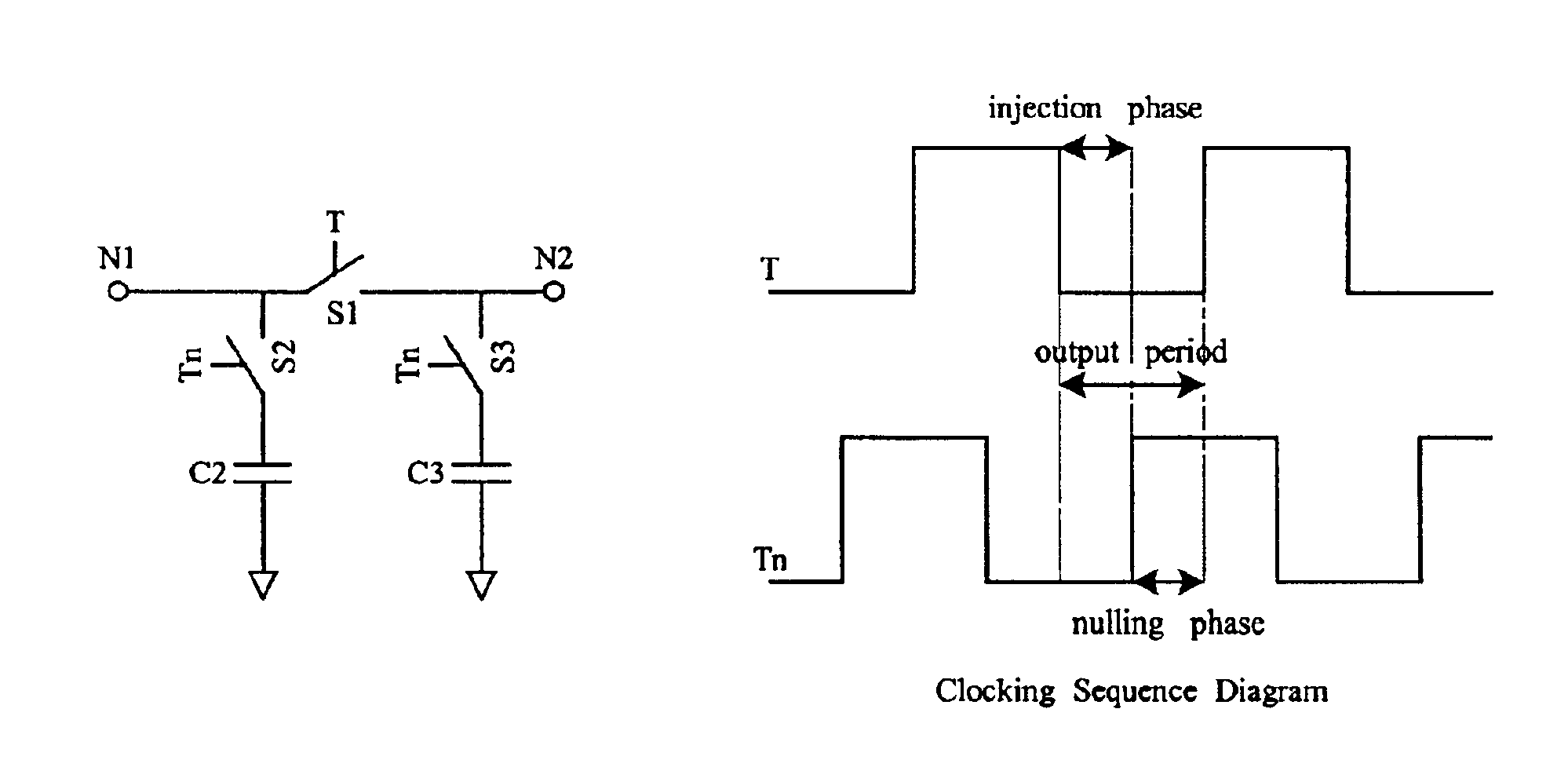
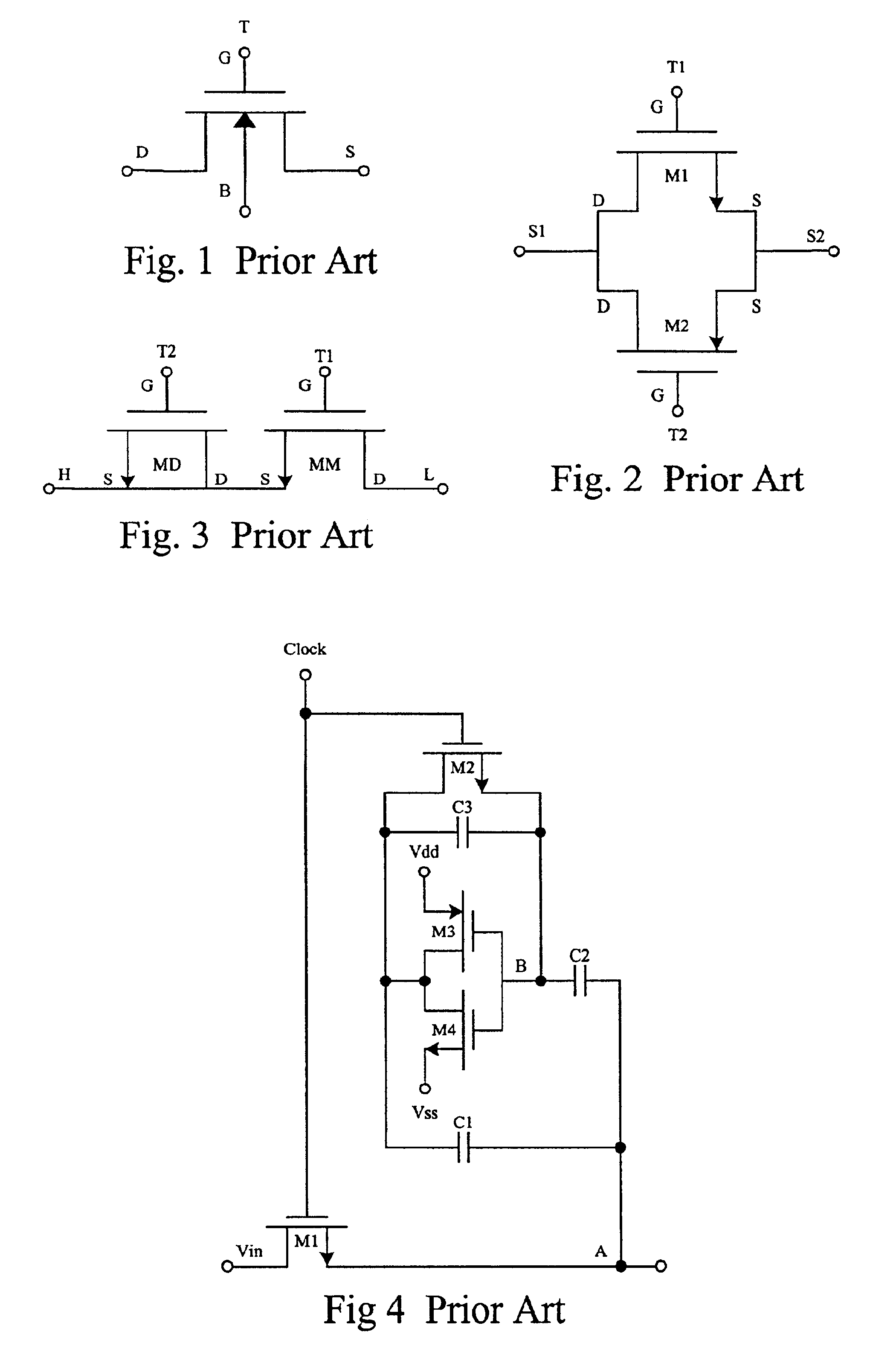
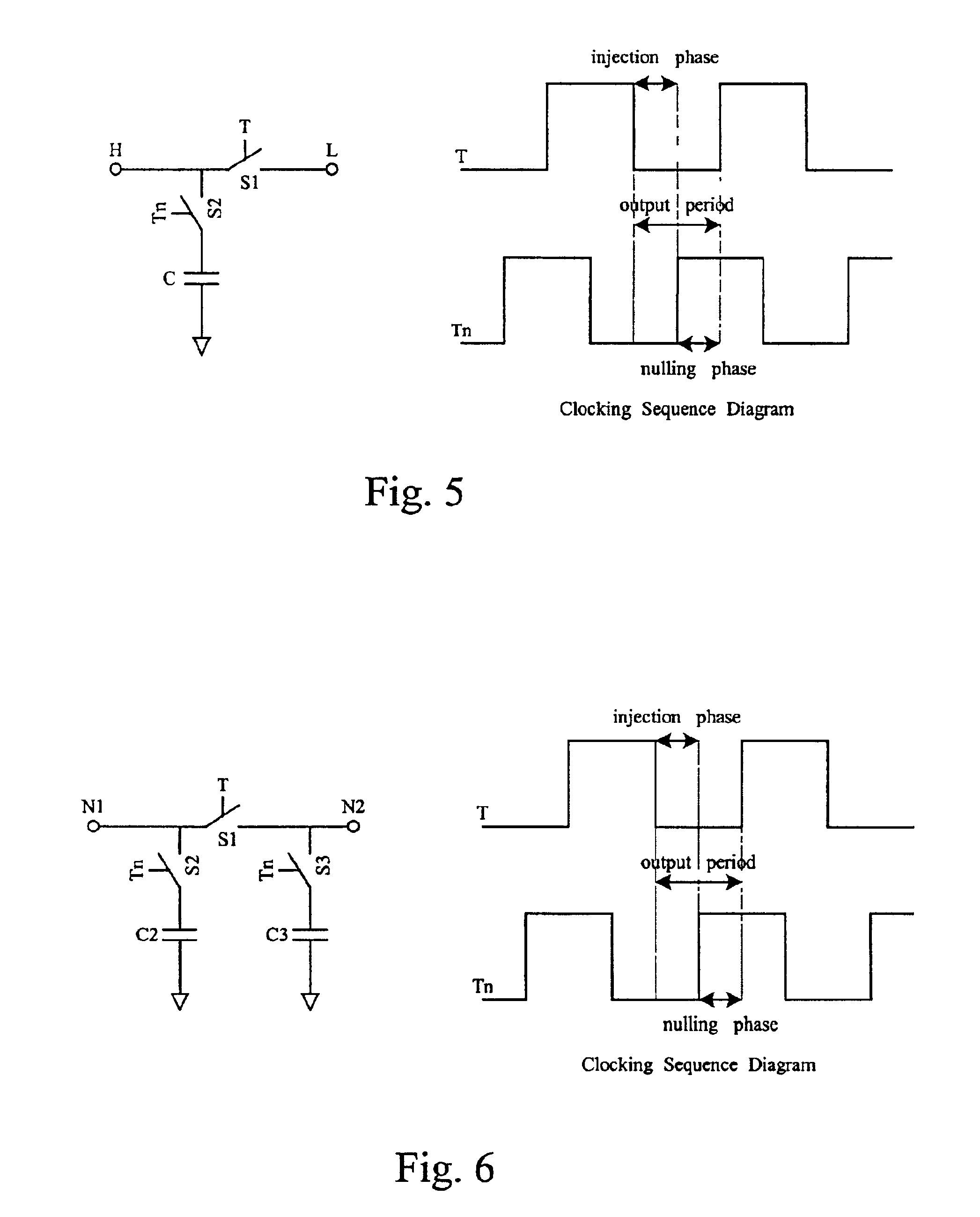
FIG. 5 illustrates an exemplary injection nulling switch of the present invention. Two switched elements, S1 and S2, are connected together at terminal H. The other terminal of switched element S2 is connected to a capacitor C, which is connected to ground or a reference voltage. The clock signals T and Tn switching the element S1 and S2, respectively, are shown in the clocking sequence diagram of FIG. 5. Terminal H is connected to the high impedance node and has a charge injection and clock feed-through error, while terminal L is connected to the low impedance node. The switched elements can be of any MOS switches described, for example, in the prior art. However, the simplest configuration is to use a single NMOS transistor for the switched element S1 and S2. The size of the switched elements can be of minimum size and the value of the capacitor C can be around 1 pF.
Operation of the circuit is based on two phases, the injection phase and the nulling phase. At the start of the inje...
PUM
 Abstract
Description
Claims
Application Information


