Fabrication of abrupt ultra-shallow junctions

a technology of ultra-shallow junctions and manufacturing methods, which is applied in the direction of semiconductor/solid-state device manufacturing, basic electric elements, electric apparatus, etc., can solve the problems of unsatisfactory needs for effective methods of forming ultra-shallow junctions, and undesirable dopants spreading, so as to facilitate the formation of very shallow junctions and fast diffusing species

Inactive Publication Date: 2005-02-08
TEXAS INSTR INC
View PDF3 Cites 100 Cited by
  • Summary
  • Abstract
  • Description
  • Claims
  • Application Information

AI Technical Summary

Benefits of technology

One aspect of the invention relates to a method of forming P-N junctions within a semiconductor substrate. The method involves providing a temporary impurity atom, such as fluorine, within the semiconductor substrate crystal matrix prior to in-diffusion of a primary dopant, such as boron. The impurity atom is a faster diffusing species relative to silicon atoms. During in-diffusion, the second dopant acts to reduce the depth to which the dopant diffuses and thereby facilitates the formation of very shallow junctions.

Problems solved by technology

The formation of ultra-shallow junctions, that is, junctions having source / drain regions no more than about 50 nm thick, is considered one of the significant challenges in manufacturing the next generation of CMOS devices.
Enhanced diffusivity causes undesirable spreading of the dopants during thermal annealing that is carried out to repair the crystal structure of the substrate after doping.
Thus, there remains an unsatisfied need for effective methods of forming ultra-shallow junctions.

Method used


Image

  • Fabrication of abrupt ultra-shallow junctions
  • Fabrication of abrupt ultra-shallow junctions
  • Fabrication of abrupt ultra-shallow junctions

Examples


Embodiment Construction

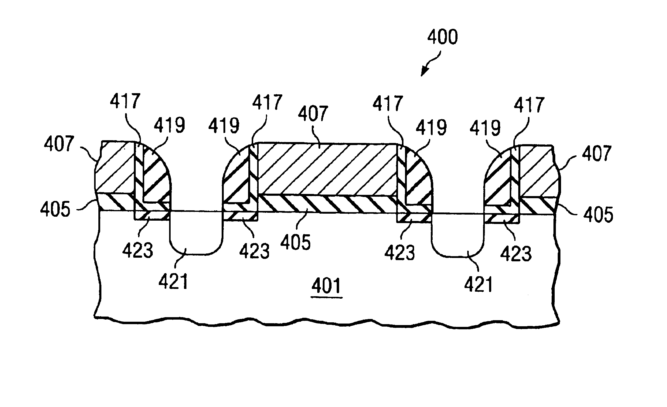
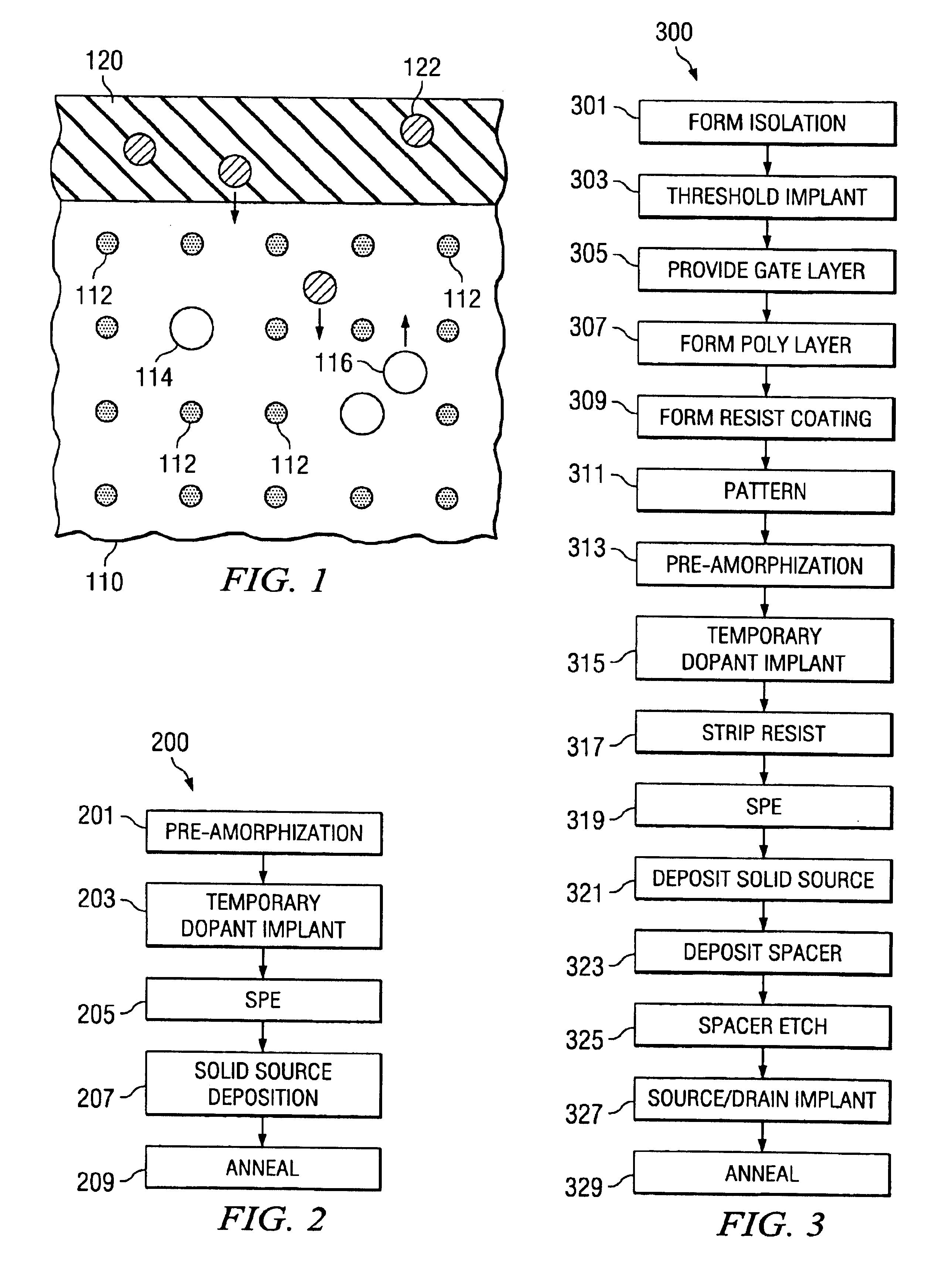
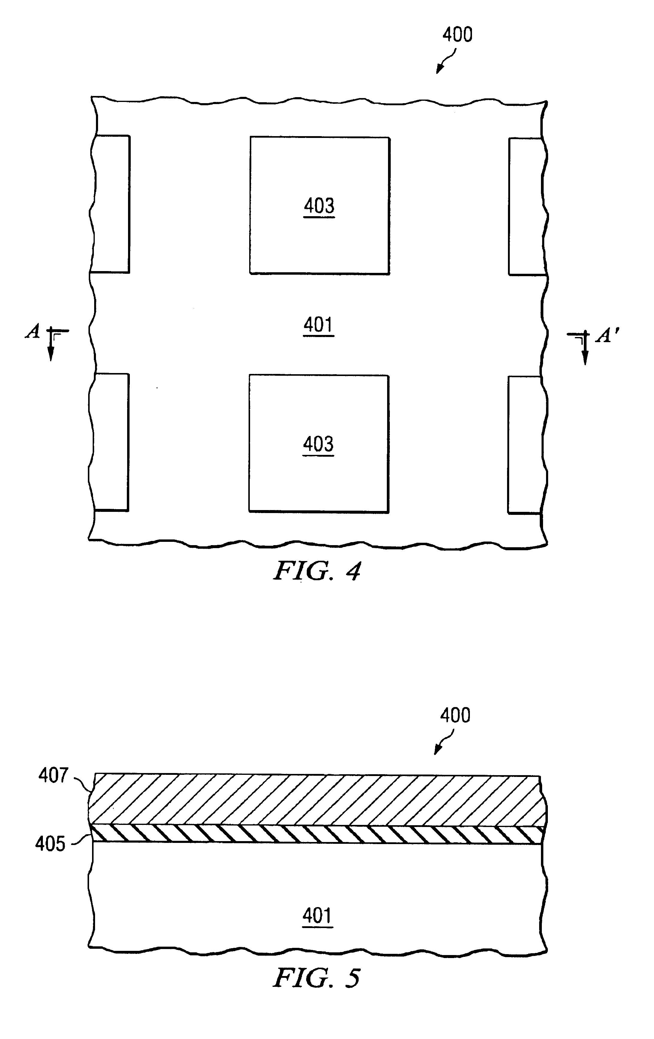
The present invention will now be described with reference to the attached drawings, wherein like reference numerals are used to refer to like elements throughout. FIG. 1 illustrates a process of the present invention. Substrate 110 comprises a single crystal of semiconductor atoms 112 in which are substituted atoms 114 of what can be referred to as a temporary dopant. Solid source 120, which comprises target dopant atoms 122, is provided as a coating over the substrate 110. During the process of the invention, the substrate 110 and the solid source 120 are heated. Heating causes a portion of the target dopant atoms 122 to enter the substrate 110, diffuse through the substrate 110, and become substituted in the crystal matrix of the substrate 110. Heating also causes a portion of the temporary dopant atoms 114 to react with interstitials within the substrate 110 and form interstitial species 116, which diffuse out of the substrate 110. The temporary dopant atoms 114 function to remo...


PUM


Abstract

One aspect of the invention relates to a method of forming P-N junctions within a semiconductor substrate. The method involves providing a temporary impurity species, such as fluorine, within the semiconductor crystal matrix prior to solid source in-diffusion of the primary dopant, such as boron. The impurity atom is a faster diffusing species relative to silicon atoms. During in-diffusion, the temporary impurity species acts to reduce the depth to which the primary dopant diffuses and thereby facilitates the formation of very shallow junctions.

Description

FIELD OF THE INVENTIONThe present invention relates generally to semiconductor device manufacturing and more particularly to methods of manufacturing devices with ultra-shallow junctions.BACKGROUND OF THE INVENTIONIn the semiconductor industry, there is a continuing trend toward high device densities. To achieve these high device densities, small features on semiconductor wafers are required. These features include source regions, drain regions, and channel regions that relate to devices, such as field effect transistors (FETs).In the process of scaling down complementary metal oxide semiconductor (CMOS) devices, which are a type of FET, a vertical dimension must be reduced at the same time as horizontal dimensions are reduced. In particular, source and drain regions, or at least source drain extension regions adjacent the channel, must be made extremely shallow, with a corresponding increase in doping, in order to avoid short channel effects. For example, the source / drain extension...

Claims


Application Information

Patent Timeline
Patent Type & Authority Patents(United States)
IPC IPC(8): H01L21/225H01L21/02
CPCH01L21/2255
Inventor CHAKRAVARTHI, SRINIVASANCHIDAMBARAM, PERIANNAN
Owner TEXAS INSTR INC
Why Eureka
Try Eureka