Method for bottomless deposition of barrier layers in integrated circuit metallization schemes

a technology of integrated circuits and barrier layers, which is applied in the direction of crystal growth process, crystal growth process, semiconductor/solid-state device details, etc., can solve the problems of negative impact on reliability and signal delay, negative impact on reliability and resistivity of conductive paths, and additional implementation difficulties, so as to avoid the deposition of barrier layers

Inactive Publication Date: 2005-02-08
INTERUNIVERSITAIR MICROELECTRONICA CENT VZW (IMEC) +2
View PDF36 Cites 114 Cited by
  • Summary
  • Abstract
  • Description
  • Claims
  • Application Information

AI Technical Summary

Benefits of technology

Desirably, the first surface is of an insulating layer and the second surface is of a conductive layer. More particularly, in the preferred embodiments, a method is described for depositing a barrier layer on part of the sidewalls of an opening passing through at least an insulating layer to a layer consisting essentially of a conductive material is described. This method comprises creating the opening in the insulating layer, conditioning at least insulating sidewalls of the opening to form ligands on these insulating sidewalls, and thereafter depositing the barrier layer on the insulating sidewalls while avoiding deposition of the barrier layer on conductive sidewalls.

Problems solved by technology

Cu can have a high diffusion in the surrounding insulating layers, which negatively affects the reliability and the signal delay.
Several problems are related to the deposition of barrier layers.
Since the adhesion between the barrier layer 16 and the underlying conductive layer 20 is not always good, the current flowing between the different conductive levels will be influenced, having a negative impact on the reliability and the resistivity of the conductive path.
This method implies a more complex process with more process steps than conventional barrier formation, which causes additional difficulties by implementation.
Furthermore, the cost will increase.

Method used


Image

  • Method for bottomless deposition of barrier layers in integrated circuit metallization schemes
  • Method for bottomless deposition of barrier layers in integrated circuit metallization schemes
  • Method for bottomless deposition of barrier layers in integrated circuit metallization schemes

Examples


Embodiment Construction

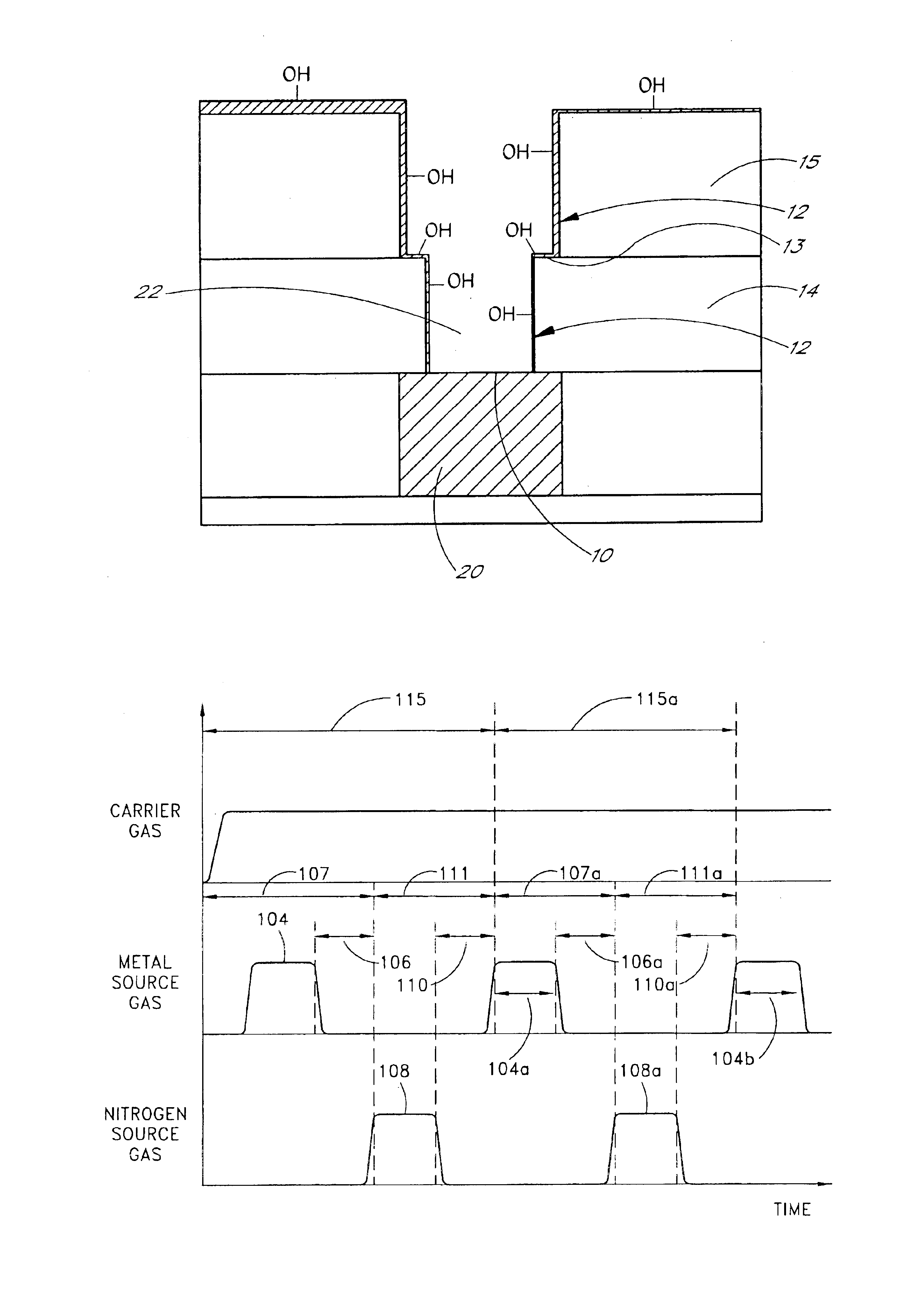
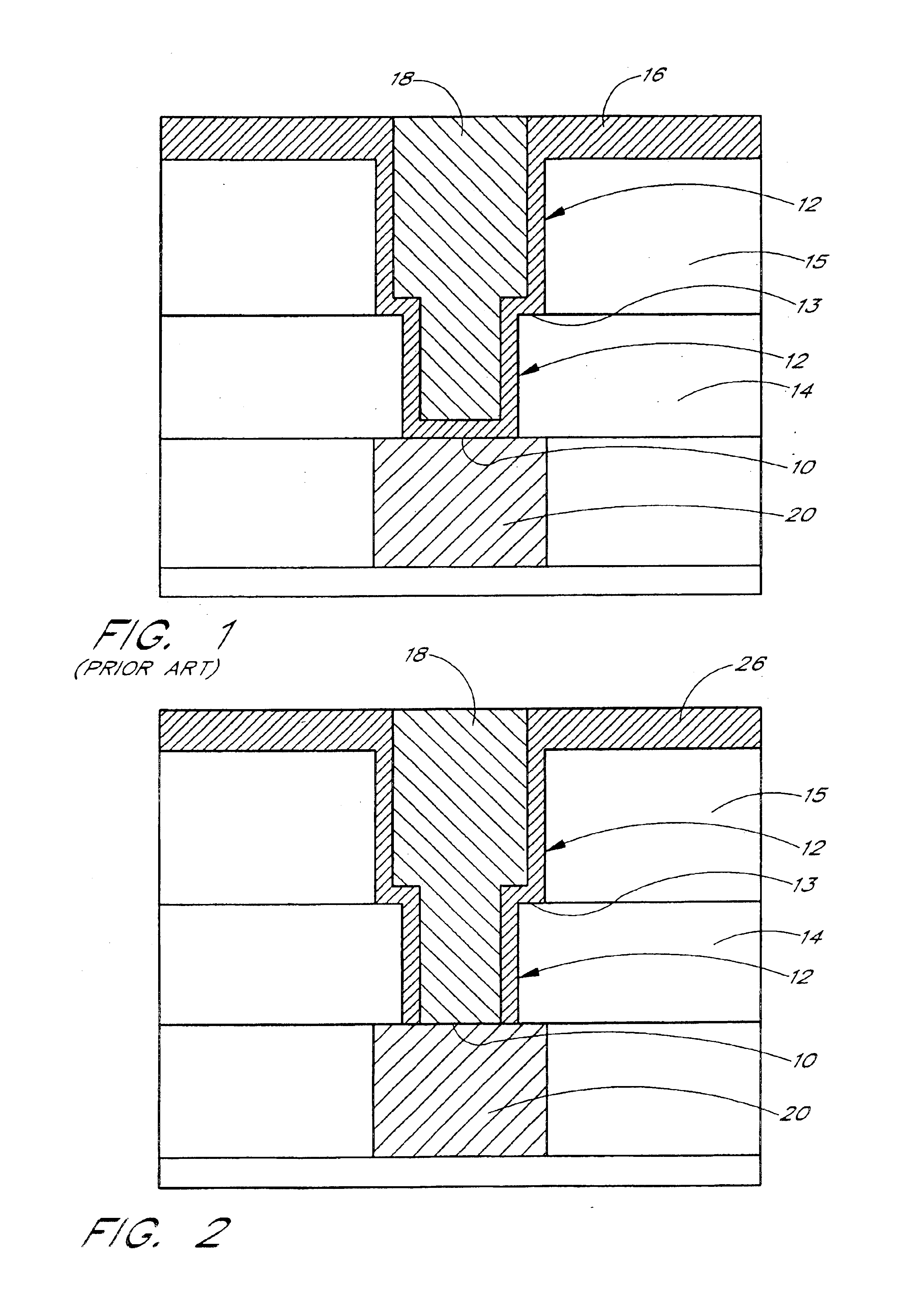
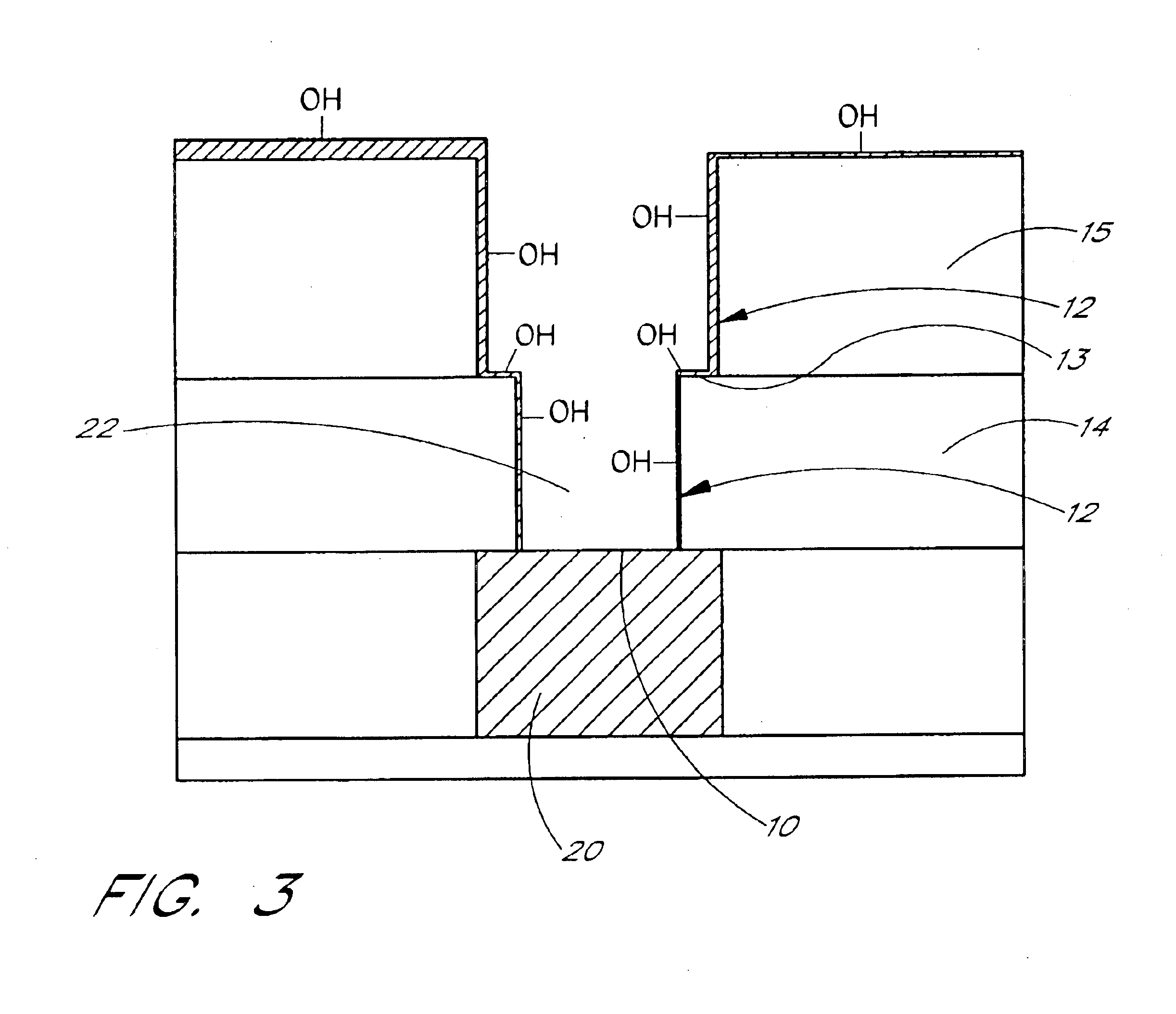
Methods for depositing a layer, preferably a barrier layer, on a substrate are described herein. The substrate includes at least a first surface and a second surface, which differ in material composition. The method preferably includes conditioning at least one of the surfaces to form ligands on the conditioned surface and thereafter depositing a barrier layer on the conditioned surface while avoiding deposition on the non-conditioned surface. Conditioning, as used herein, prepares the surface for further deposition, and in the illustrated embodiment involves making the surface susceptible to an atomic layer deposition (ALD) process to form the desired barrier layer. In contrast, the non-conditioned surface is substantially insensitive to the ALD process for the desired barrier layer. The “non-conditioned” surface can be achieved by failure to condition this surface or by further modification of conditioning on this surface.

While illustrated in the context of selective barrier depos...


PUM

PropertyMeasurementUnit
temperatureaaaaaaaaaa
Pressureaaaaaaaaaa

Abstract

Methods are disclosed for selective deposition on desired materials. In particular, barrier materials are selectively formed on insulating surfaces, as compared to conductive surfaces. In the context of contact formation and trench fill, particularly damascene and dual damascene metallization, the method advantageously lines insulating surfaces with a barrier material. The selective formation allows the deposition to be “bottomless,” thus leaving the conductive material at a via bottom exposed for direct metal-to-metal contact when further conductive material is deposited into the opening after barrier formation on the insulating surfaces. Desirably, the selective deposition is accomplished by atomic layer deposition (ALD), resulting in highly conformal coverage of the insulating sidewalls in the opening.

Description

FIELD OF THE INVENTIONThe method relates generally to integrated circuit processing and fabrication and, more particularly, to metal interconnect structures and the deposition of barrier layers in a selective way.BACKGROUND OF THE INVENTIONThe ongoing focus on miniaturization and the increasing complexity and speed requirements of integrated circuits demand continuously higher density integration. To achieve this, there is an ongoing downscaling in the dimensions of the active devices, as well as of the structures interconnecting these devices. These interconnect structures can comprise multiple metal levels which are, depending on the desired interconnect pattern, either separated from one another by means of interlevel insulating layers or connected to one another by means of a conductive connection through the insulating layer. Besides this downscaling of the dimensions, additional measures are required to be able to meet the stringent speed specifications. Conventionally, the me...

Claims


Application Information

Patent Timeline
Patent Type & Authority Patents(United States)
IPC IPC(8): C23C16/06C23C16/04C23C16/08C23C16/02C23C16/32C30B25/02C23C16/44H01L21/70H01L21/285H01L21/02H01L23/522H01L23/532H01L23/52H01L21/768C23C16/455H01L21/205
CPCH01L23/53252H01L23/5329H01L23/53242H01L23/53238H01L23/53223H01L23/5226H01L23/53295C23C16/0272C23C16/045C23C16/08C23C16/32C23C16/44C23C16/45525C30B25/02H01L21/28562H01L21/76807H01L21/76814H01L21/76831H01L21/76838H01L21/76844H01L21/76876C30B29/02C30B29/36H01L2924/0002H01L2924/00H01L21/203
Inventor SATTA, ALESSANDRAMAEX, KARENELERS, KAI-ERIKSAANILA, VILLE ANTEROSOININEN, PEKKA JUHAHAUKKA, SUVI P.
Owner INTERUNIVERSITAIR MICROELECTRONICA CENT VZW (IMEC)
Why Eureka
Try Eureka