High temperature interface layer growth for high-k gate dielectric

a high-temperature, gate dielectric technology, applied in the direction of superimposed coating process, capacitor, coating, etc., can solve the problems of increased cost, increased cost, increased cost, etc., and achieve the effect of facilitating the production of a higher quality layer and high quality

Inactive Publication Date: 2005-02-08
PACIFIC SEISMIC PRODS +1
View PDF5 Cites 133 Cited by
  • Summary
  • Abstract
  • Description
  • Claims
  • Application Information

AI Technical Summary

Problems solved by technology

Recently, however, electrical and physical limitations have been reached in the thickness of gate dielectrics formed of SiO2.
Making the gate dielectric layer 30 thinner, however, has other effects, which may lead to performance tradeoffs, particularly where the gate dielectric 30 is SiO2.
This problem is exacerbated by conventional limitations in the ability to deposit or grow such thin films with uniform thickness.
The presence of this interfacial oxide layer 30b increases the effective oxide thickness, reducing the effectiveness of the alternative gate dielectric approach.
In addition, the interface 30b generally has unsatisfied bonds that act as interface charging centers, causing interface states.
The high density of such interface states in the low quality oxide 30b results in carrier mobility degradation in operation of the transistor 6′, where the higher the density of the interface states, the more the resulting mobility degradation.
Additionally, lower quality oxides may also suffer from issues related to, among other things, charge scattering, charge trapping, fixed charge, density of interface state (Dit), carrier mobility, etc.
Growing oxides at higher temperatures produces higher quality oxides, but the oxide growth rate is difficult to control as the oxidation occurs rapidly at higher temperatures.
Difficulty in controlling oxide growth rates can lead to non-uniform oxides, to oxides that are too thick, or to other undesirable results.

Method used


Image

  • High temperature interface layer growth for high-k gate dielectric
  • High temperature interface layer growth for high-k gate dielectric
  • High temperature interface layer growth for high-k gate dielectric

Examples


Embodiment Construction

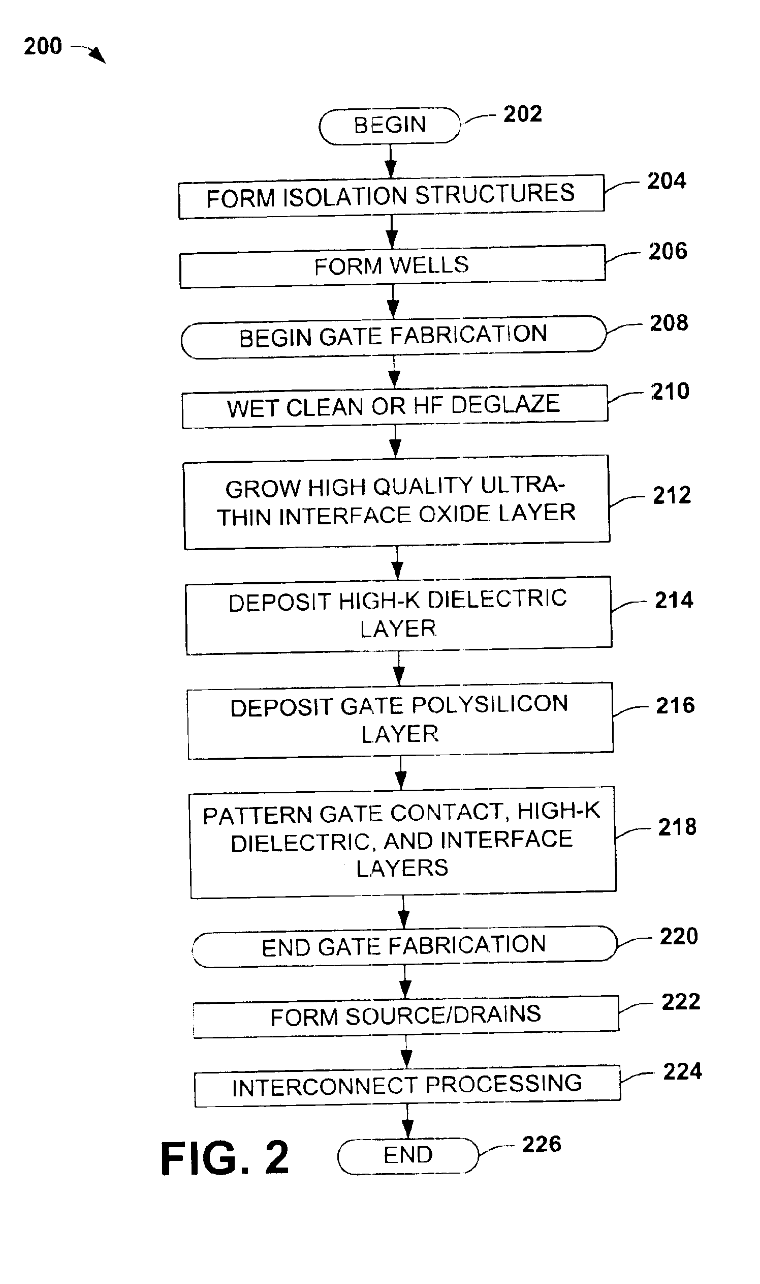
"d_n">[0021]FIG. 2 is a flow diagram illustrating an exemplary method in accordance with the present invention;

[0022]FIG. 3 is a graph charting an interface oxide layer growth rate as a function of the partial pressure of a reducing agent in a gas phase; and

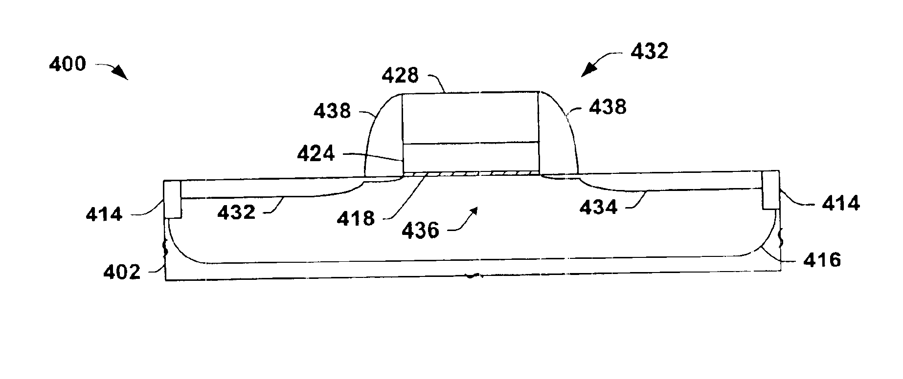
[0023]FIGS. 4-9 are partial side elevation views in section illustrating an exemplary semiconductor device being processed at various stages of manufacturing in accordance with various aspects of the invention.

DETAILED DESCRIPTION OF THE INVENTION

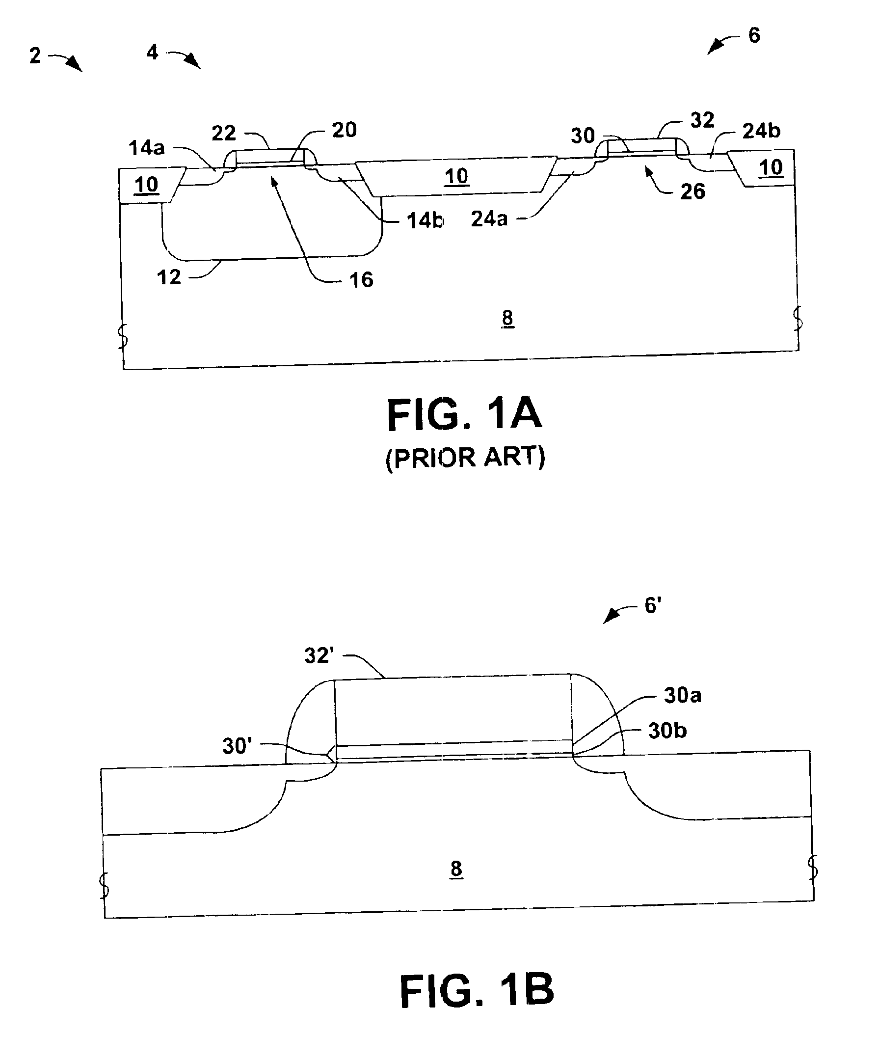
[0024]One or more implementations of the present invention will now be described with reference to the attached drawings, wherein like reference numerals are used to refer to like elements throughout. The invention relates to formation of ultra thin interface oxides suitable for implementation in gate structures in semiconductor devices, and more particularly to growing the interface oxides at high temperatures while controlling the rate of growth of the oxides (which traditionally speed...


PUM

PropertyMeasurementUnit
temperatureaaaaaaaaaa
thicknessaaaaaaaaaa
partial pressureaaaaaaaaaa

Abstract

The present invention pertains to methods for forming high quality thin interface oxide layers suitable for use with high-k gate dielectrics in the manufacture of semiconductor devices. An ambient that contains oxygen and a reducing agent is utilized to grow the layers. The oxygen facilitates growth of the layers, while the reducing agent simultaneously counteracts that growth. The rate of growth of the layers can thus be controlled by regulating the partial pressure of the reducing agent, which is the fraction of the reducing agent in the gas phase times the total pressure. Controlling and slowing the growth rate of the layers facilitates production of the layers to thicknesses of about 10 Angstroms or less at temperatures of about 850 degrees Celsius or more. Growing the layers at high temperatures facilitates better bonding and production of higher quality layers, which in turn yields better performing and more reliable resulting products.

Description

FIELD OF INVENTION[0002]The present invention relates generally to semiconductor processing, and more particularly to a methodology for establishing high quality, very thin interface layers suitable for use with high-k gate dielectrics in the manufacture of semiconductor devices.BACKGROUND OF THE INVENTION[0003]Field effect transistors (FETs) are widely used in the electronics industry for switching, amplification, filtering, and other tasks related to both analog and digital electrical signals. Most common among these are metal-oxide-semiconductor field-effect transistors (MOSFETs), wherein a metal or polysilicon gate contact is energized to create an electric field in a channel region of a semiconductor body, by which current is allowed to conduct between a source region and a drain region of the semiconductor body. The source and drain regions are typically formed by adding dopants to targeted regions on either side of the channel region in a semiconductor substrate. A gate diele...

Claims


Application Information

Patent Timeline
Patent Type & Authority Patents(United States)
IPC IPC(8): H01L21/02H01L21/28H01L29/40H01L29/51H01L21/316C23C28/00H01L29/78
CPCC23C28/00H01L21/02255H01L21/28176H01L21/28185H01L21/28194H01L21/28202H01L21/28211H01L21/31155H01L21/31662H01L21/31691H01L29/513H01L21/02238H01L29/518H01L28/56H01L29/517
Inventor COLOMBO, LUIGICHAMBERS, JAMES J.ROTONDARO, ANTONIO L. P.VISOKAY, MARK R.
Owner PACIFIC SEISMIC PRODS
Why Eureka
Try Eureka