Scanning charged particle microscope

Inactive Publication Date: 2005-02-08
SII NANOTECHNOLOGY INC
View PDF7 Cites 49 Cited by
  • Summary
  • Abstract
  • Description
  • Claims
  • Application Information

AI Technical Summary

Benefits of technology

[0008]The present invention provides a rapid control function capable of extrapolating an in-focus point from image information for a singl

Problems solved by technology

However, in this method, there is a problem in that a pattern extending in a vertical direction of the sample image as shown in FIG. 1A is necessary in order to implement automatic focal point adjustment.
If this is not present, it is not possible to perform a comparison of every scanning line.
Therefore, when the image is a linear pattern going along the direction of the scanning lines as

Method used


Image

  • Scanning charged particle microscope
  • Scanning charged particle microscope
  • Scanning charged particle microscope

Examples


Embodiment Construction

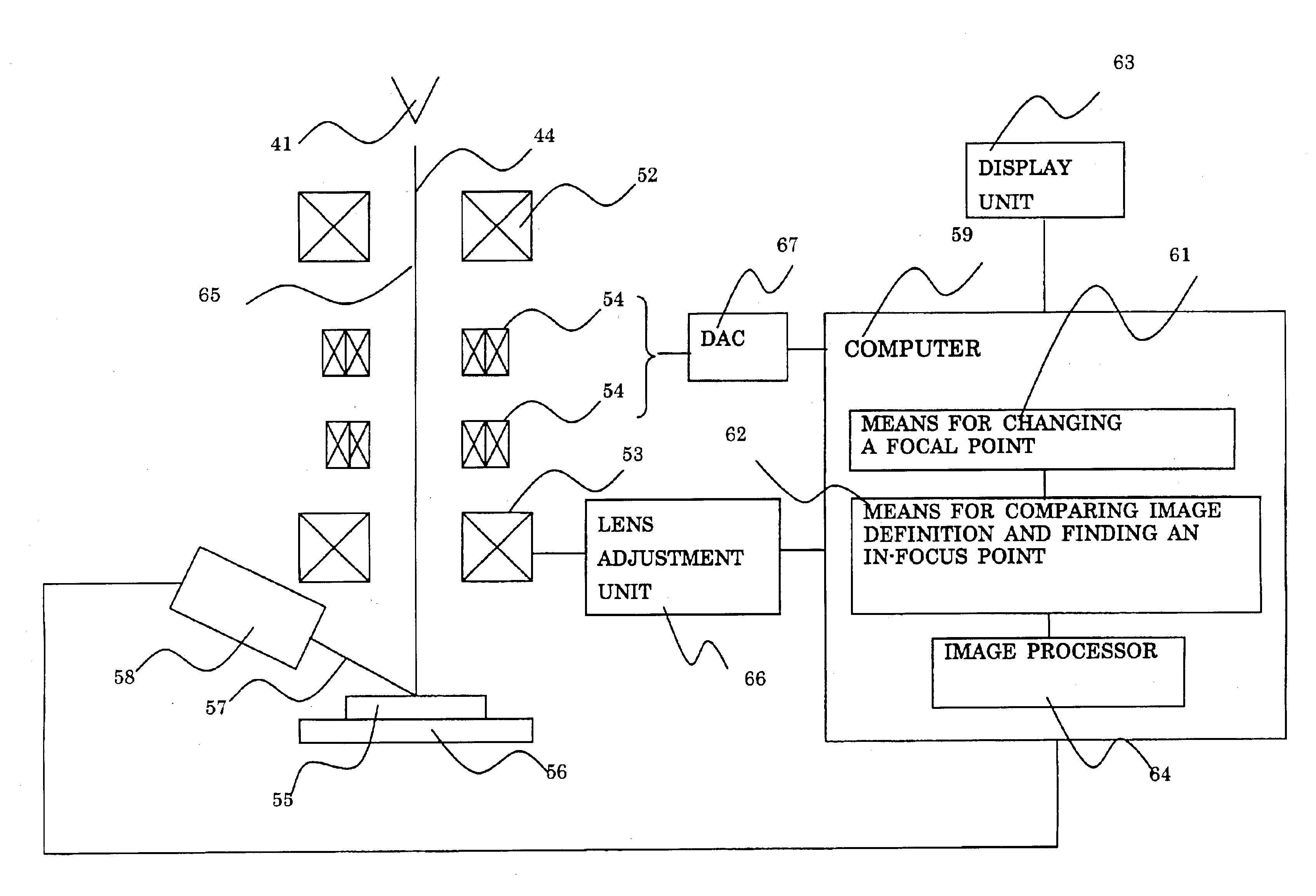
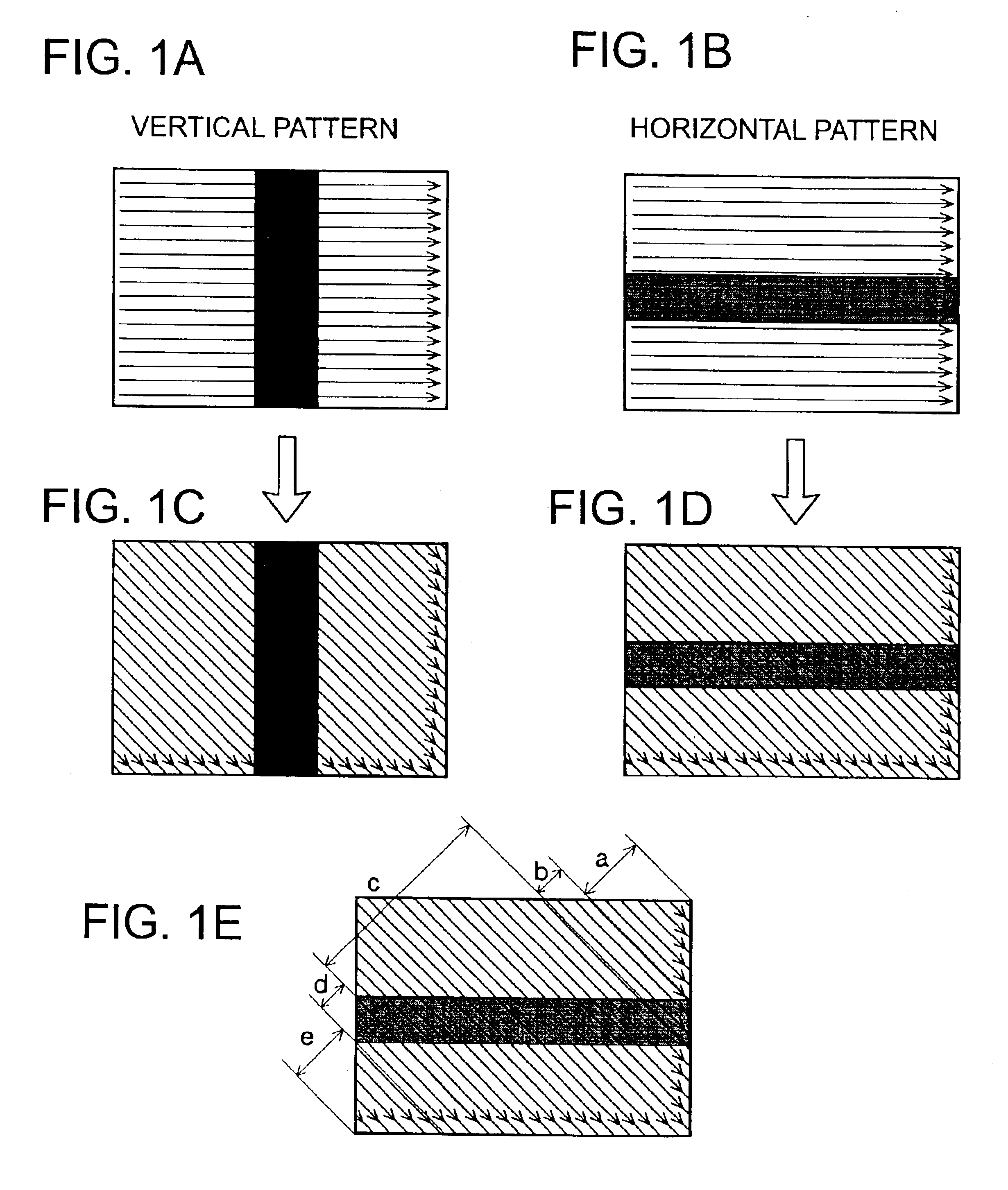
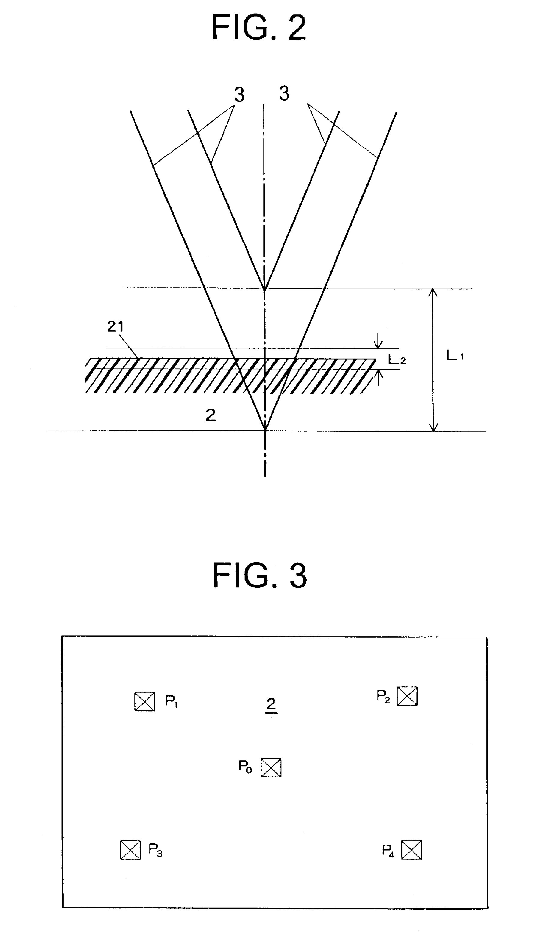
[0018]The present invention provides a technology for performing more detailed checks using an electron microscope for defects such as those caused by foreign bodies becoming attached to some of the same chips arrayed in a lattice on a semiconductor wafer that are detected using a defect checking device, and as such it is important to acquire clearly defined images of defects constituting the subjects of such checks. The situation in the related art where related autofocusing methods were used to perform frame focusing control on image information for a plurality of frames was excessively time-consuming whatever the approach adopted. A method where the focal point is changed for every horizontal scanning line which switches vertical deflection so that image definition is compared for every scanning line to exert focusing control is therefore preferred. However, there is still occasionally the inconvenience that this does not operate very well with images for regions where the patter...


PUM


Abstract

The present invention sets out to provide a scanning charged particle microscope equipped with a rapid control function capable of extrapolating an in-focus point from image information for a single frame and an automatic focusing system capable of reliably and precisely carrying out a focusing operation for a horizontal pattern image. The automatic focusing system provided in the scanning charged particle microscope of the present invention is provided with means for changing a focal point each raster scan line, and control means for comparing image information each scanning line and extrapolating focusing positions. The scanning line can then be made to be an inclined scanning line that is a combination of a horizontal component and a vertical component with respect to a chip array on a semiconductor wafer. Further, a method is adopted comprising a first step of reliably taking in a coarse in-focus point and a second step of detecting the in-focus point with a high degree of precision.

Description

BACKGROUND OF THE INVENTION[0002]1. Field of the Invention[0003]The present invention relates to a method and system for reliably, accurately and rapidly executing an automatic focusing function for a scanning charged particle microscope typified by an electron microscope, etc.[0004]2. Description of Related Art[0005]Tests are implemented using defect checking devices to detect defects such as the adhesion of foreign matter that are the main cause of defective device operation as a means of managing yield in semiconductor device manufacturing processes. The defect checking devices detect defects and store the number and position of these defects in a defect file for subsequent processes. Semiconductor device wafers are typically substantially circular plates as shown in FIG. 4. A lattice of a large number of the same chips 2 are transferred onto a single wafer 1. The checking device then scans the surface of the wafer manufactured in this manner using an optical probe so as to detec...

Claims


Application Information

Patent Timeline
IPC IPC(8): G02B7/28G01N23/225G02B7/36G21K7/00H01J37/21H01J37/28
CPCG01N23/225H01J37/21H01J37/28H01J2237/216H01J2237/2817
Inventor SUZUKI, HIDEKAZUUEMOTO, ATSUSHI
Owner SII NANOTECHNOLOGY INC
Why Eureka
Try Eureka