

Semiconductor device including multiple field effect transistors, with first FETs having oxide spacers and the second FETs having oxide nitride oxidation protection
- Summary
- Abstract
- Description
- Claims
- Application Information
AI Technical Summary
Benefits of technology
Problems solved by technology
Method used
Image

Examples
first embodiment
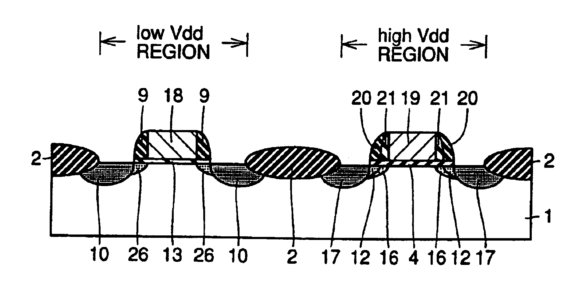
Referring to FIG. 1, in a 2-power supply semiconductor device including a plurality of field transistors according to a first embodiment of the invention, there are formed, on a main surface of a p type semiconductor substrate 1, a first field effect transistor supplied with a first power supply voltage (low Vdd) and a second field effect transistor supplied with a second voltage (high Vdd) higher than the first power supply voltage, spaced apart from each other. An isolation oxide film 2 is formed between the first and second field effect transistors.
In the low Vdd region, there are formed, on the main surface of substrate 1, a pair of first source / drain regions 10, and a pair of low concentration, impurity diffusion regions 8 adjacent thereto, spaced apart from each other and having a first channel region therebetween. Low concentration, n type impurity diffusion region 8 formed adjacent to the first channel region and high concentration, n type impurity diffusion region 10 formed...
second embodiment
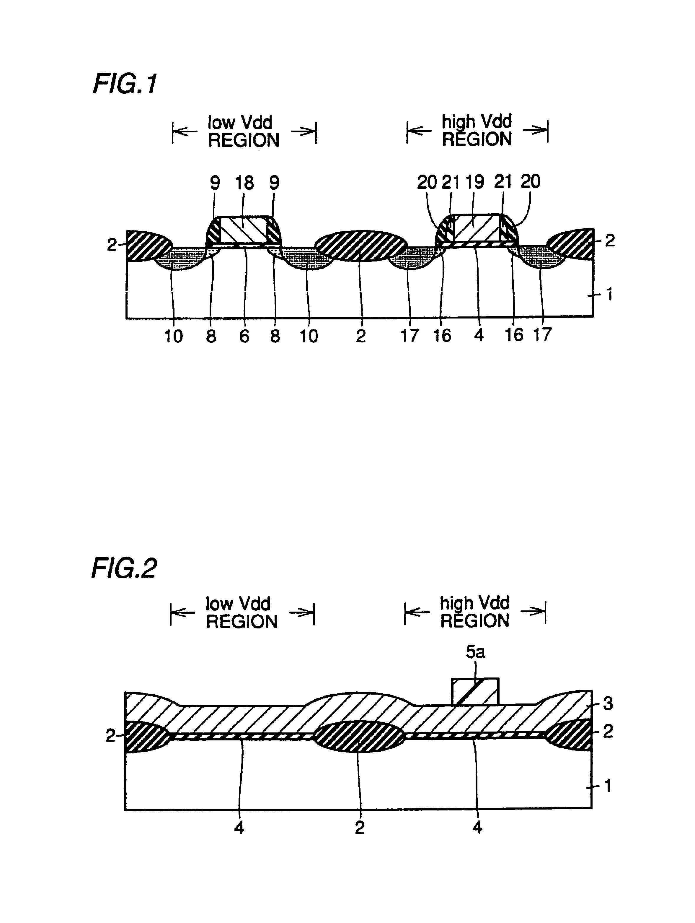
Referring to FIG. 11, in a 2-power supply semiconductor device including a plurality of field transistors according to a second embodiment of the invention, there are formed, on a main surface of a p type semiconductor substrate 1, a first field effect transistor supplied with a first power supply voltage (low Vdd) and a second field effect transistor supplied with a second voltage (high Vdd) higher than the first power supply voltage, spaced apart from each other. An isolation oxide film 2 is formed between the first and second field effect transistors.
In the low Vdd region, there are formed, on the main surface of substrate 1, a pair of first source / drain regions 10 and a pair of impurity diffusion regions 26, spaced apart from each other and having a first channel region therebetween. Intermediate concentration, n type impurity diffusion region 26 formed adjacent to the first channel region and high concentration, n type impurity diffusion region 10 formed adjacent to n type impu...
third embodiment
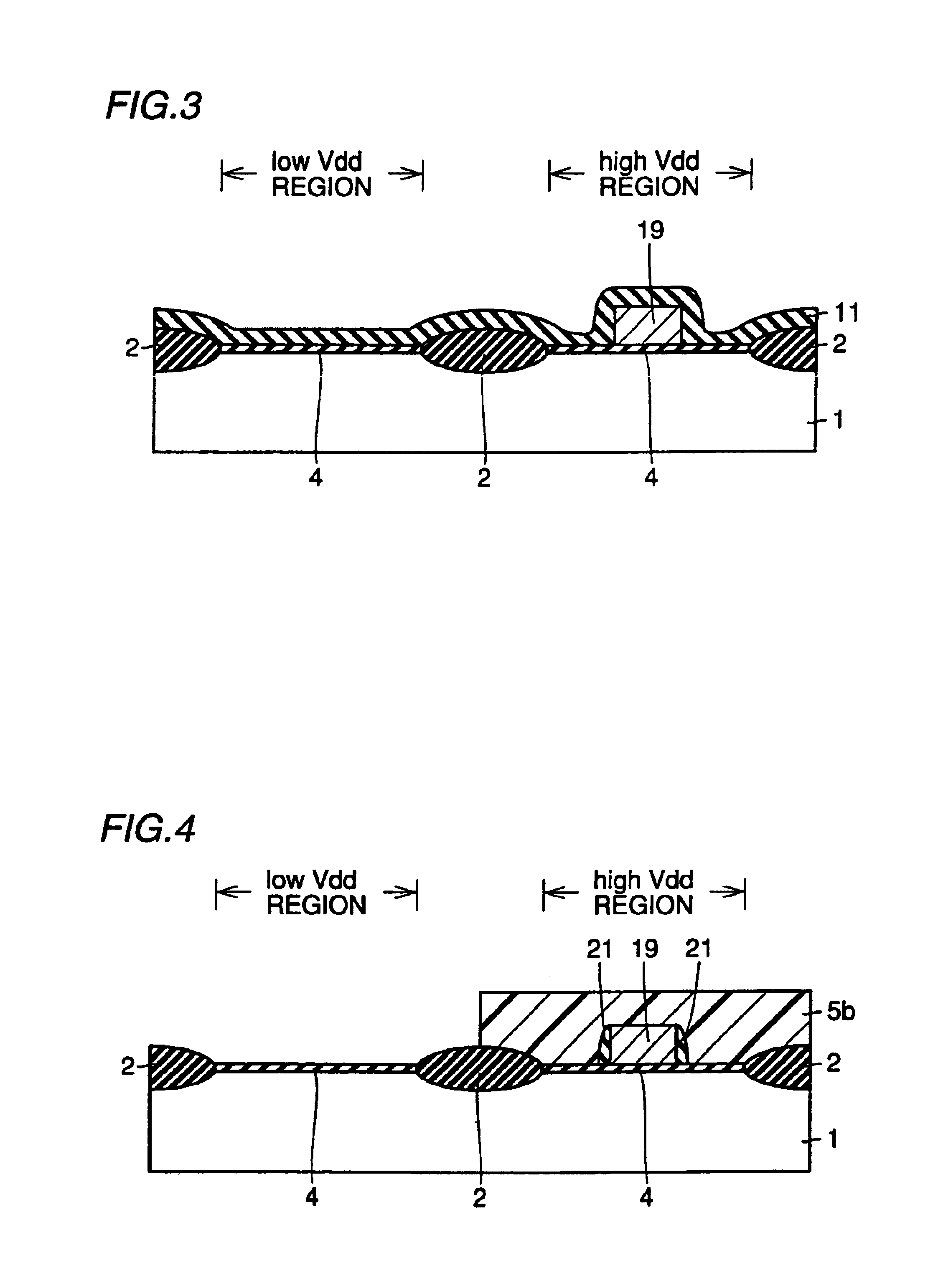
Referring to FIG. 22, in a 2-power supply semiconductor device including a plurality of field transistors according to a third embodiment of the invention, there are formed, on a main surface of a p type semiconductor substrate 1, a first field effect transistor supplied with a first power supply voltage (low Vdd) and a second field effect transistor supplied with a second voltage (high Vdd) higher than the first power supply voltage, spaced apart from each other. An isolation oxide film 2 is formed between the first and second field effect transistors.
In the low Vdd region, there are formed, on the main surface of substrate 1, a pair of first source / drain regions 10, and a pair of impurity diffusion regions 8, spaced apart from each other and having a first channel region. Low concentration, n type impurity diffusion region 8 formed adjacent to the first channel region and high concentration, n type impurity diffusion region 10 formed adjacent to n type impurity region 8 constitute...
PUM
 Abstract
Description
Claims
Application Information