Thin film transfer, organic electroluminescence display device and manufacturing method of the same
- Summary
- Abstract
- Description
- Claims
- Application Information
AI Technical Summary
Benefits of technology
Problems solved by technology
Method used
Image

Examples
Embodiment Construction
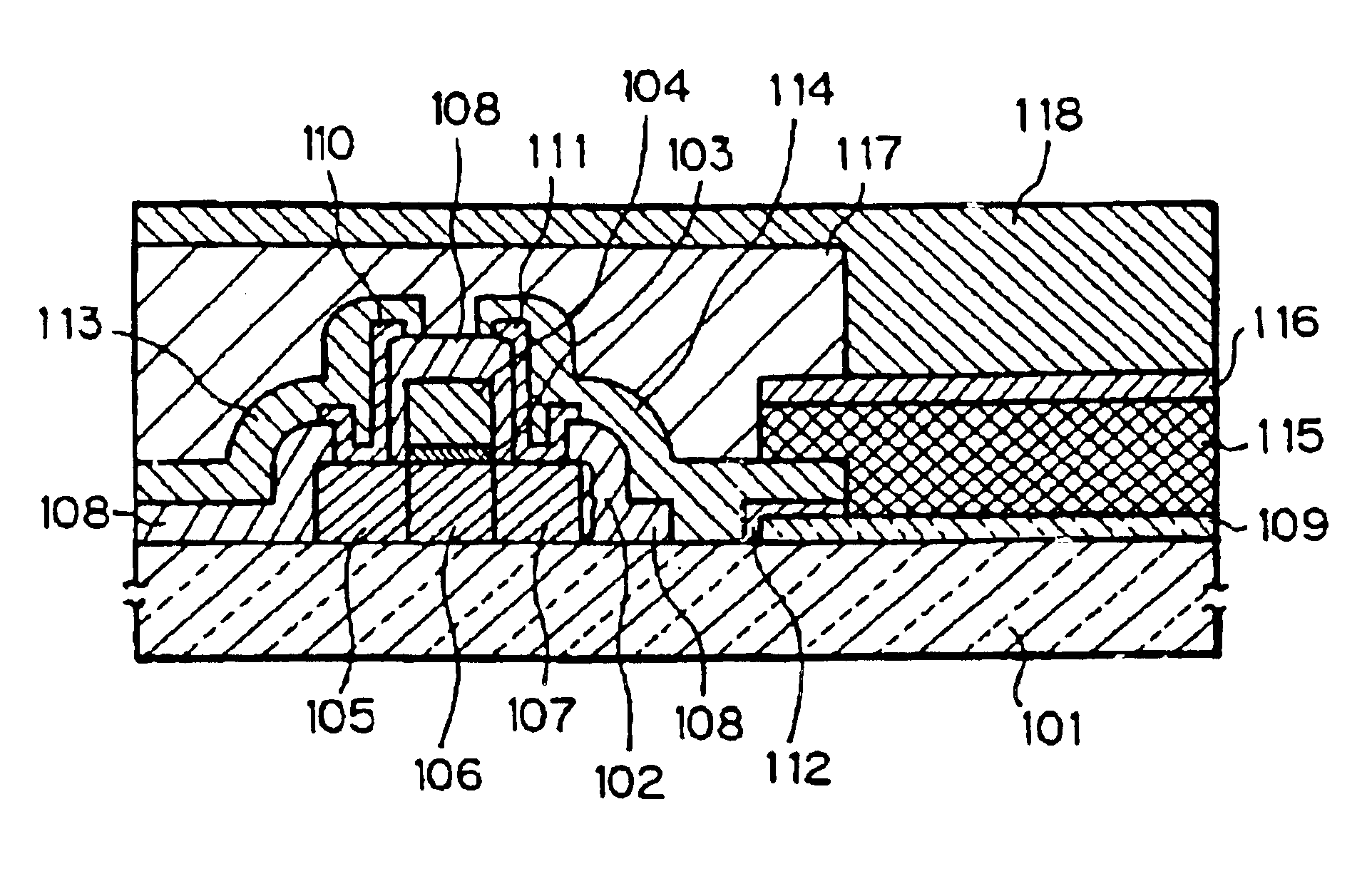
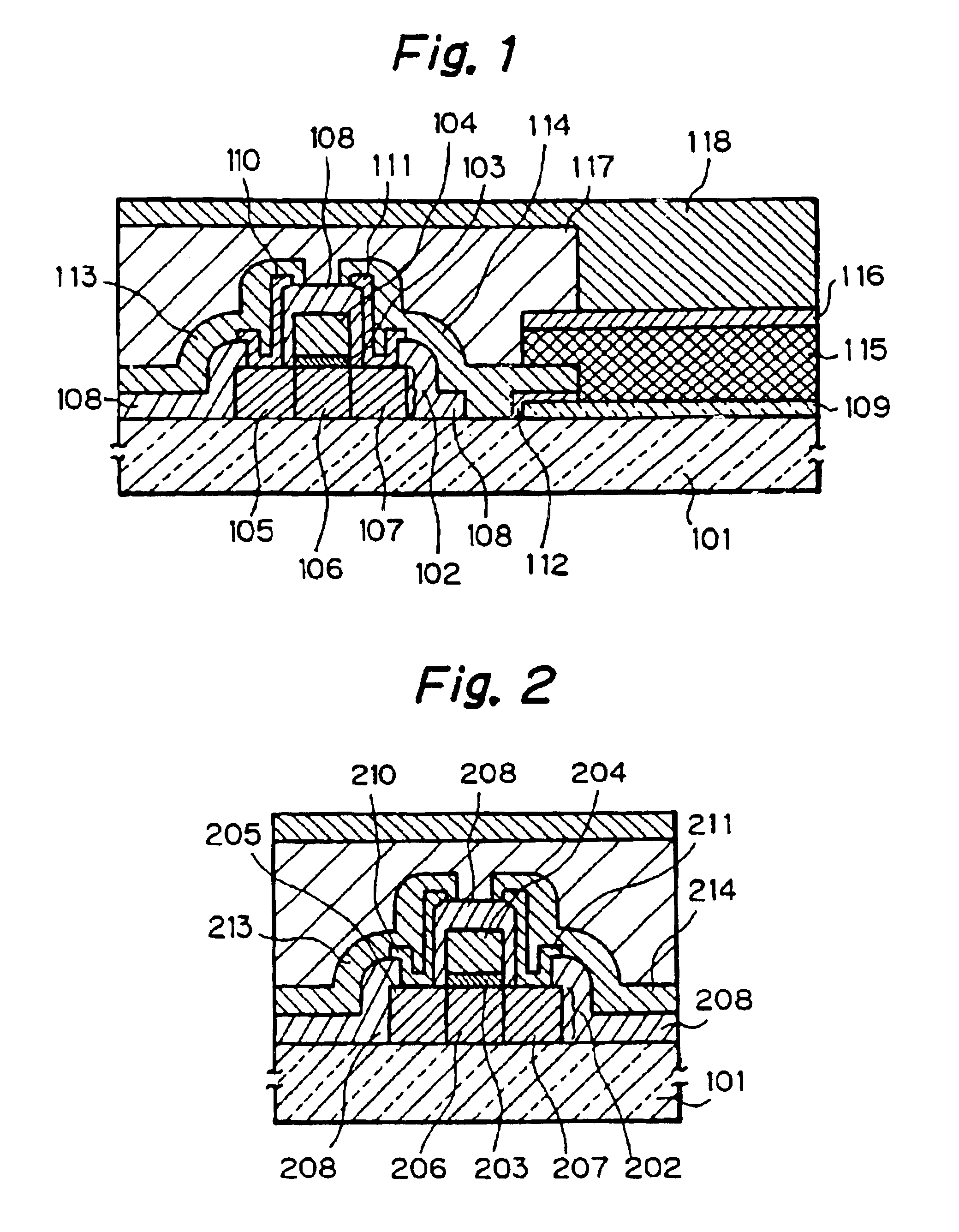
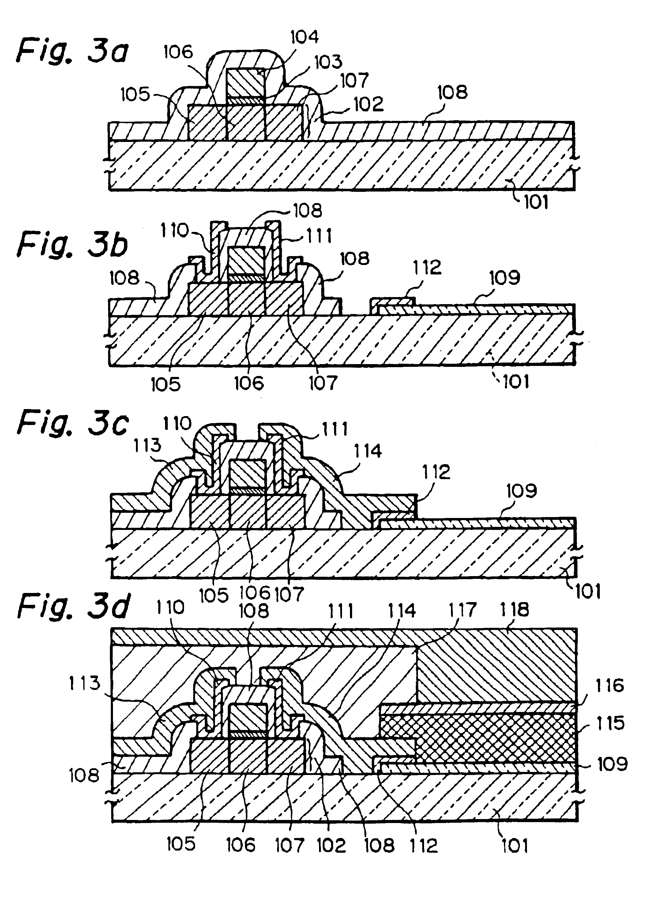
FIG. 1 shows an organic electroluminescence (EL) element and a current control thin film transistor for controlling current applied to the EL element in a preferred embodiment of an organic EL display device according to the present invention.
In FIG. 1, a reference numeral 101 denotes a transparent substrate such as a quartz substrate. On the substrate 101, many of the organic EL elements and their peripheral circuit elements such as current control thin film transistors, switching thin film transistors for switching the respective current control transistors, another thin film transistors which constitute peripheral driving circuits and capacitors are formed.
Each of the current control thin film transistors is substantially constituted by an active silicon layer 102 formed on the substrate 101, a gate oxide layer of SiO2 103 formed on a central region of the active silicon layer 102, a gate electrode of phosphorous doped Polysilicon 104 laminated on the gate oxide layer 103, a sour...
PUM
 Abstract
Description
Claims
Application Information
 - Generate Ideas
- Intellectual Property
- Life Sciences
- Materials
- Tech Scout
- Unparalleled Data Quality
- Higher Quality Content
- 60% Fewer Hallucinations
Browse by: Latest US Patents, China's latest patents, Technical Efficacy Thesaurus, Application Domain, Technology Topic, Popular Technical Reports.
© 2025 PatSnap. All rights reserved.Legal|Privacy policy|Modern Slavery Act Transparency Statement|Sitemap|About US| Contact US: help@patsnap.com