Plasma display panel having grooves in the dielectric layer
a dielectric layer and display panel technology, applied in the field of plasma display panels, can solve the problems of error discharge and crosstalk, poor exhaust, and reduced luminance, and achieve the effect of preventing luminance from being reduced and improving exhaust ability
- Summary
- Abstract
- Description
- Claims
- Application Information
AI Technical Summary
Benefits of technology
Problems solved by technology
Method used
Image
Examples
first embodiment
As shown in FIGS. 4a and 4b, a plasma display panel according to a first embodiment of the present invention includes first substrate electrode pairs (sustain electrodes) with a Y electrode 41 and a Z electrode 42, formed on a first substrate in one direction, first barriers 43 formed on a second substrate at constant intervals to cross the first substrate electrode pairs, auxiliary barriers 43a formed on both sides of the first barriers 43, and second barriers 43b formed on the second substrate corresponding to a region between the respective first substrate electrode pairs. The second barriers 43b have a width which increases toward the first barriers 43 and are symmetrical toward the first substrate electrode pairs at their adjacent both sides. A reference numeral 51 denotes a main discharge region.
As described above, both sides of the second barriers 43b are separated from adjacent first barriers 43 without closely contacting each other, so that a path is formed. This path is us...
second embodiment
As shown in FIG. 8, a plasma display panel according to the second embodiment of the present invention includes a first substrate 110 and a second substrate 120 which are combined with each other in parallel at a constant interval.
First substrate electrode pairs(sustain electrodes) 111 for sustaining light-emission of the cell are formed below the first substrate 110. A black matrix is provided between the first substrate 110 and the first substrate electrode pairs 111. The first substrate electrode pairs 111 and the black matrix are sealed by a dielectric layer 112 and a passivation layer 113 formed by plasticity.
Stripe type barriers 121 on which a phosphor layer 123 is deposited are formed on the second substrate 120. A plurality of projections 130 are formed between the barriers 121 at constant intervals. At this time, the projections 130 are preferably arranged between the barriers 121 corresponding to the boundary portion between the cells. A top portion at both sides of the pr...
third embodiment
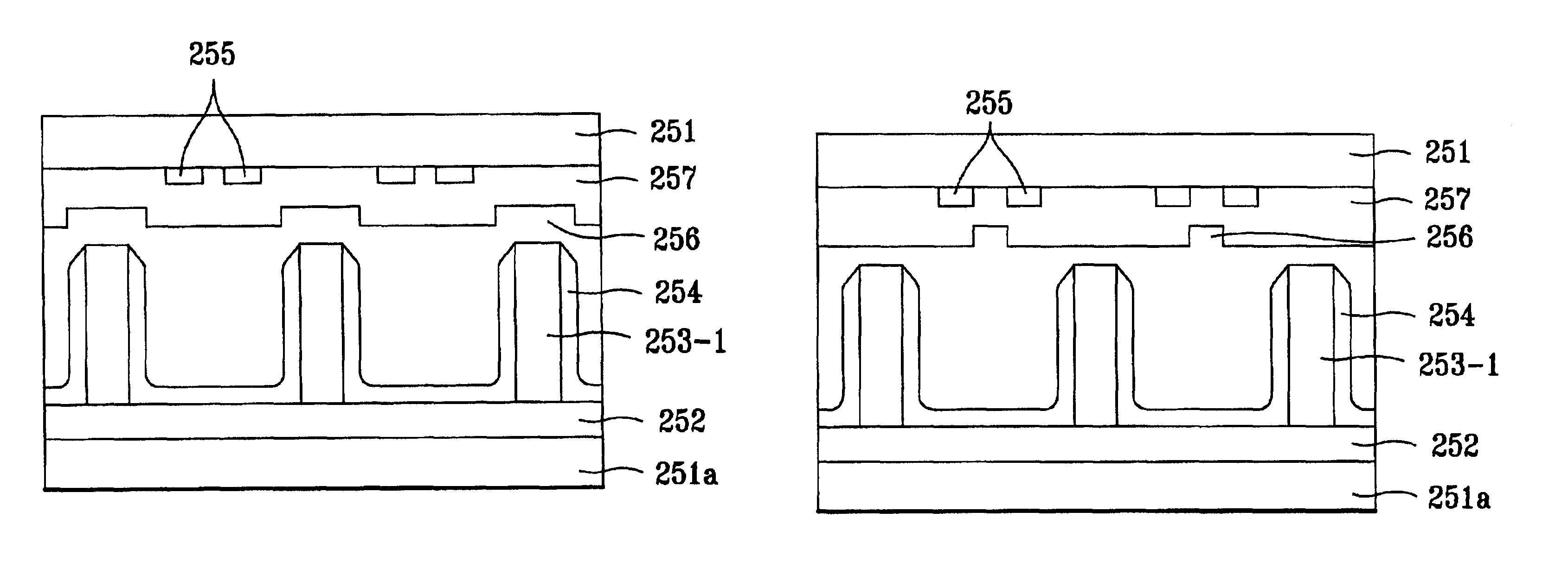
As shown in FIG. 11, a plasma display panel according to the third embodiment of the present invention includes a first substrate 251, a second substrate 251a, a plurality of first substrate electrode pairs 255 formed on the first substrate 251 at constant intervals, second substrate electrodes 259 (not shown) formed on the second substrate 251a, a second dielectric layer 252 formed on the second substrate 251a including the second substrate electrodes 259, lattice shaped barriers 253(253-1, 253-2) formed on the second dielectric layer 252 to cross in horizontal and vertical directions, a phosphor layer 254 formed on the second dielectric layer 252 including the barriers 253(253-1, 253-2), and a first dielectric layer 257 formed on an entire surface of the first substrate 251 including the first substrate electrode pairs 255, having a groove 256 of a predetermined depth in a region corresponding to vertical barriers 253-1 among the barriers 253(253-1, 253-2) along a direction in whi...
PUM
 Abstract
Description
Claims
Application Information
 - R&D
- Intellectual Property
- Life Sciences
- Materials
- Tech Scout
- Unparalleled Data Quality
- Higher Quality Content
- 60% Fewer Hallucinations
Browse by: Latest US Patents, China's latest patents, Technical Efficacy Thesaurus, Application Domain, Technology Topic, Popular Technical Reports.
© 2025 PatSnap. All rights reserved.Legal|Privacy policy|Modern Slavery Act Transparency Statement|Sitemap|About US| Contact US: help@patsnap.com


