Test interconnect having suspended contacts for bumped semiconductor components

a technology of interconnection and bumped semiconductor components, which is applied in the direction of individual semiconductor device testing, measurement instrument housing, instruments, etc., can solve the problems of difficult reliable electrical connection, easy deformation of contacts during handling, and the size of bumped contacts on a component can vary

Inactive Publication Date: 2005-02-08
MICRON TECH INC
View PDF66 Cites 58 Cited by
  • Summary
  • Abstract
  • Description
  • Claims
  • Application Information

AI Technical Summary

Benefits of technology

In accordance with the present invention, an improved interconnect for testing bumped semiconductor components, a method for fabricating the interconnect, and test systems incorporating the interconnect, are provided. The interconnect includes a substrate and a plurality of flexible contacts on the substrate for electrically engaging bumped contacts on a component under test. The interconnect also includes conductors formed on surfaces of the substrate, and conductive vias formed within the substrate, in electrical communication with the flexible contacts and with external contacts on the substrate.

Problems solved by technology

One problem with making these temporary electrical connections is that the sizes of the bumped contacts on a component can vary.
The interconnect contacts may not be able to accommodate these size differences, making reliable electrical connections difficult to make.
This problem is compounded because the interconnect contacts must penetrate native oxide layers on the bump contacts to make low resistance electrical connections.
Another problem with bumped contacts particularly solder balls, is that the contacts deform easily during handling and testing, especially at elevated temperatures.
For performing test procedures, it may be difficult to make low resistance electrical connections with deformed contacts.
Specifically, the contacts on the interconnect may not adequately engage and penetrate the surfaces of the bumped contacts unless large contact forces are employed.
However, the large contact forces can also deform the bumped contacts.
For subsequent bonding procedures, deformed contacts can make alignment and bonding of the component with a mating substrate more difficult.
In addition, deformed contacts are a cosmetic problem that can adversely affect a users perception of a semiconductor component.

Method used


Image

  • Test interconnect having suspended contacts for bumped semiconductor components
  • Test interconnect having suspended contacts for bumped semiconductor components
  • Test interconnect having suspended contacts for bumped semiconductor components

Examples


Embodiment Construction

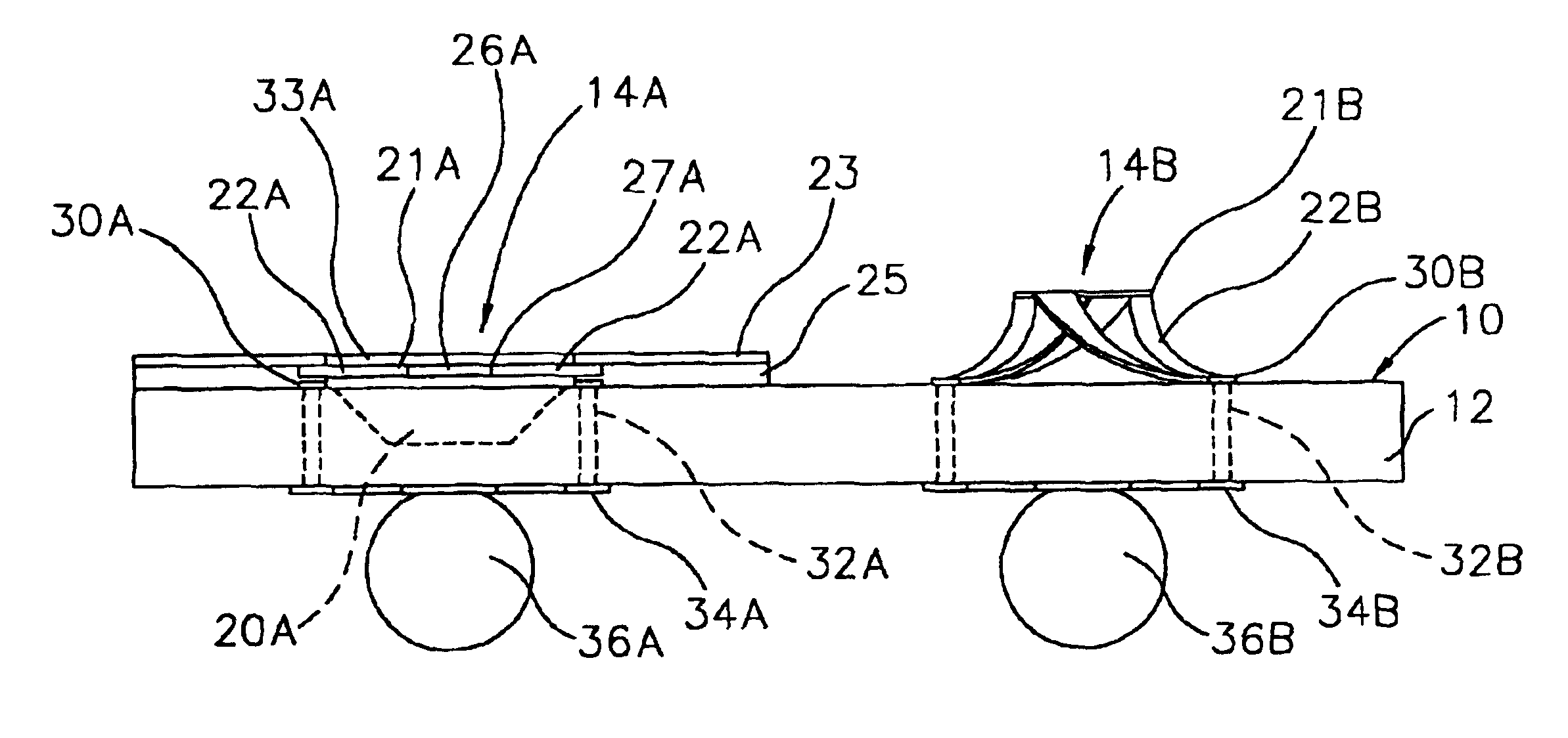
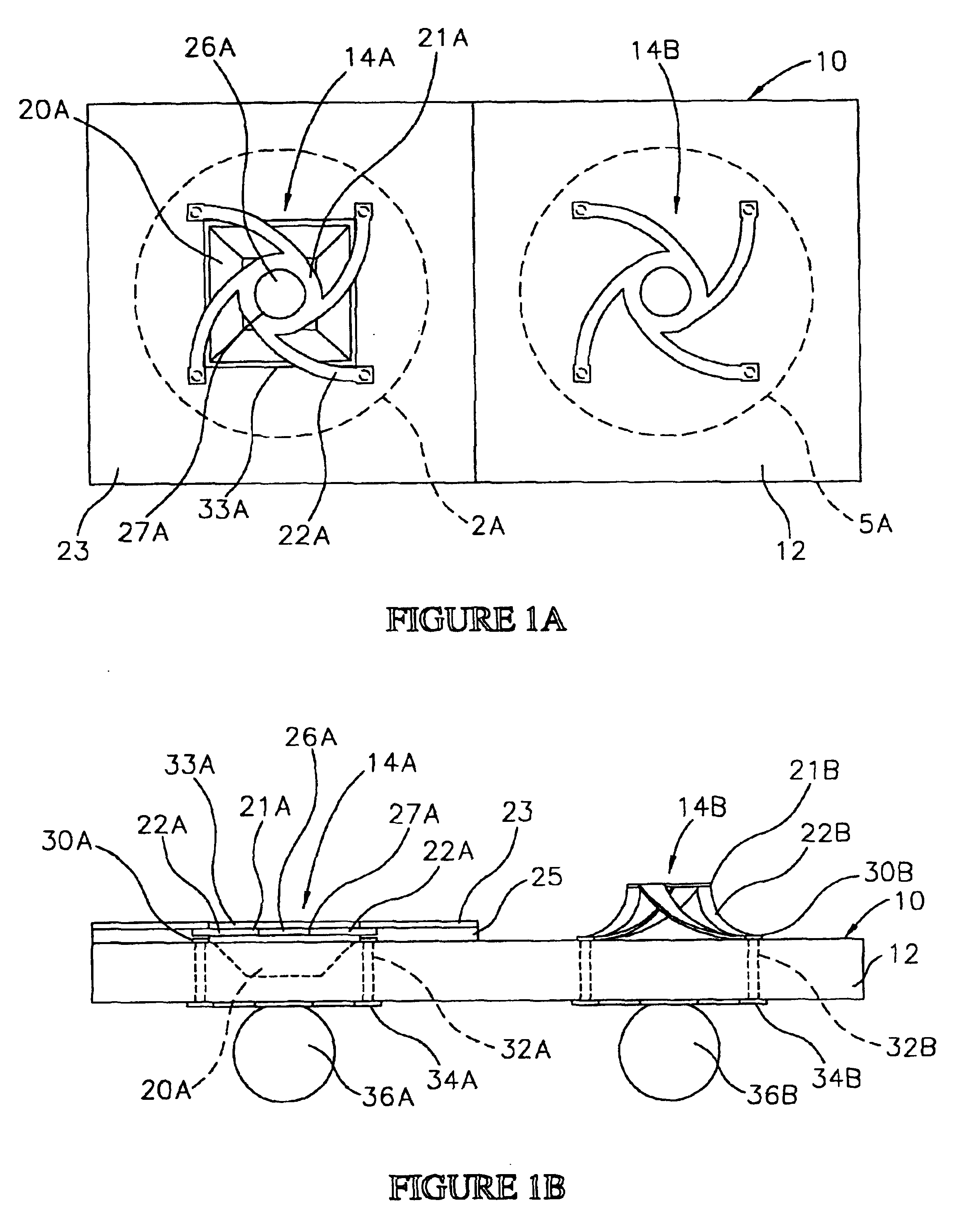
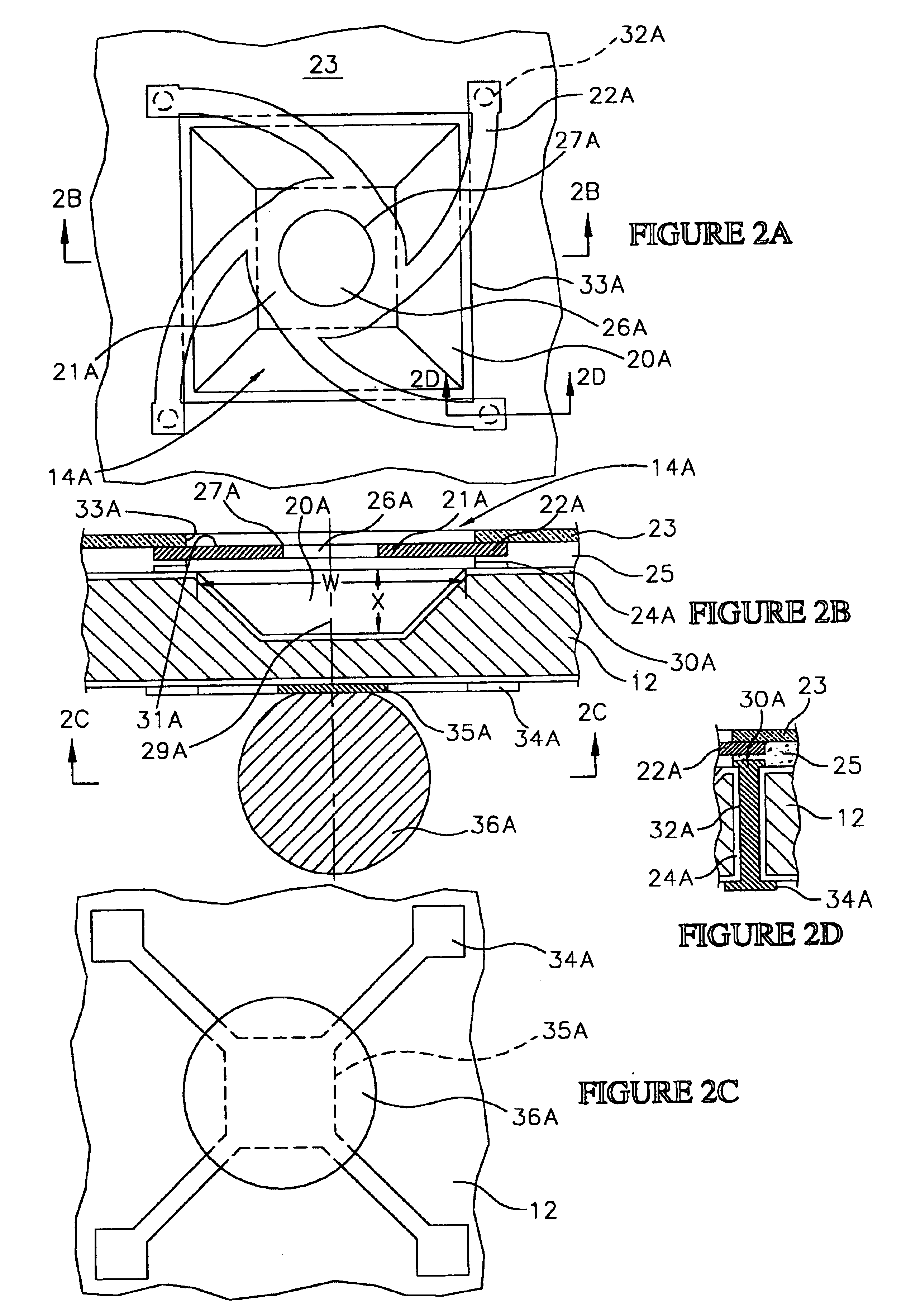
Referring to FIG. 1A, an interconnect 10 constructed in accordance with the invention is illustrated. The interconnect 10 includes a substrate 12, and a pattern of contacts 14A or 14B formed on the substrate 12. The contacts 14A or 14B are adapted to electrically engage bumped contacts 16 (FIG. 3A) formed on land pads 28 (FIG. 3A) on a semiconductor component 18 (FIG. 3A).

As used herein, the term “semiconductor component” refers to an electronic component that includes a semiconductor die. Exemplary semiconductor components include bare semiconductor dice, chip scale packages, ceramic or plastic semiconductor packages, BGA devices, semiconductor wafers, and panels containing multiple chip scale packages.

For illustrative purposes, two different contact embodiments are illustrated in FIG. 1. However, in actual practice the interconnect 10 will contain only one type of contact, either contact 14A, or contact 14B. Also for illustrative purposes, only one contact for each embodiment is i...


PUM

PropertyMeasurementUnit
widthaaaaaaaaaa
depthaaaaaaaaaa
angleaaaaaaaaaa

Abstract

An interconnect for testing semiconductor components includes a substrate, and contacts on the substrate for making temporary electrical connections with bumped contacts on the components. Each contact includes a recess and a support member over the recess configured to electrically engage a bumped contact. The support member is suspended over the recess on spiral leads formed on a surface of the substrate. The spiral leads allow the support member to move in a z-direction within the recess to accommodate variations in the height and planarity of the bumped contacts. In addition, the spiral leads twist the support member relative to the bumped contact to facilitate penetration of oxide layers thereon. The spiral leads can be formed by attaching a polymer substrate with the leads thereon to the substrate, or by forming a patterned metal layer on the substrate. In an alternate embodiment contact, the support member is suspended over the surface of the substrate on raised spring segment leads.

Description

FIELD OF THE INVENTIONThis invention relates generally to the manufacture and testing of semiconductor components. More particularly, this invention relates to an interconnect for electrically engaging bumped semiconductor components.BACKGROUND OF THE INVENTIONSemiconductor components, such as bare dice, chip scale packages, BGA devices and wafers can include terminal contacts in the form of bumped contacts. This type of component is sometimes referred to as a “bumped” component (e.g., bumped die, bumped wafer).The bumped contacts provide a high input / output capability for a component, and permit the component to be surface mounted, or alternately flip chip mounted, to a mating substrate, such as a printed circuit board (PCB). Typically, the bumped contacts comprise solder balls, which permits the components to be bonded to the mating substrate using a solder reflow process. For some components, such as chip scale packages and BGA devices, the bumped contacts can be arranged in a de...

Claims


Application Information

Patent Timeline
Patent Type & Authority Patents(United States)
IPC IPC(8): G01R1/067G01R3/00G01R1/073H05K3/32G01R1/04
CPCG01R1/0466G01R1/06738G01R3/00G01R1/07314G01R1/07378Y10T29/49165H05K3/326Y10T29/49156Y10T29/49126Y10T29/49155
Inventor FARNWORTH, WARREN M.AKRAM, SALMAN
Owner MICRON TECH INC
Why Eureka
Try Eureka