Method for detecting geometrical-optical aberrations
a technology of optical aberration and geometric aberration, applied in the direction of instruments, electrical devices, material analysis, etc., can solve problems such as distortion of probe profiles, and achieve the effect of adequate resolution
- Summary
- Abstract
- Description
- Claims
- Application Information
AI Technical Summary
Benefits of technology
Problems solved by technology
Method used
Image
Examples
Embodiment Construction
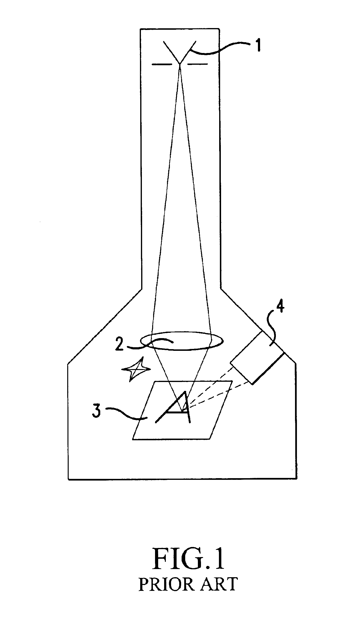
The exemplary embodiment of the invention shown in FIG. 1 is a scanning electron microscope, in which electrons are emitted from a source 1, usually an approximately punctiform tungsten tip, and are guided by lenses 2, such as electrical and / or magnetic multipoles, line by line over the object 3 to be imaged, as indicated by the arrows. The electrons radiated back by the object 3, or the secondary electrons emitted from it the object 3, are registered by a suitable detector 4, which registers an image in the form of a brightness or intensity distribution.
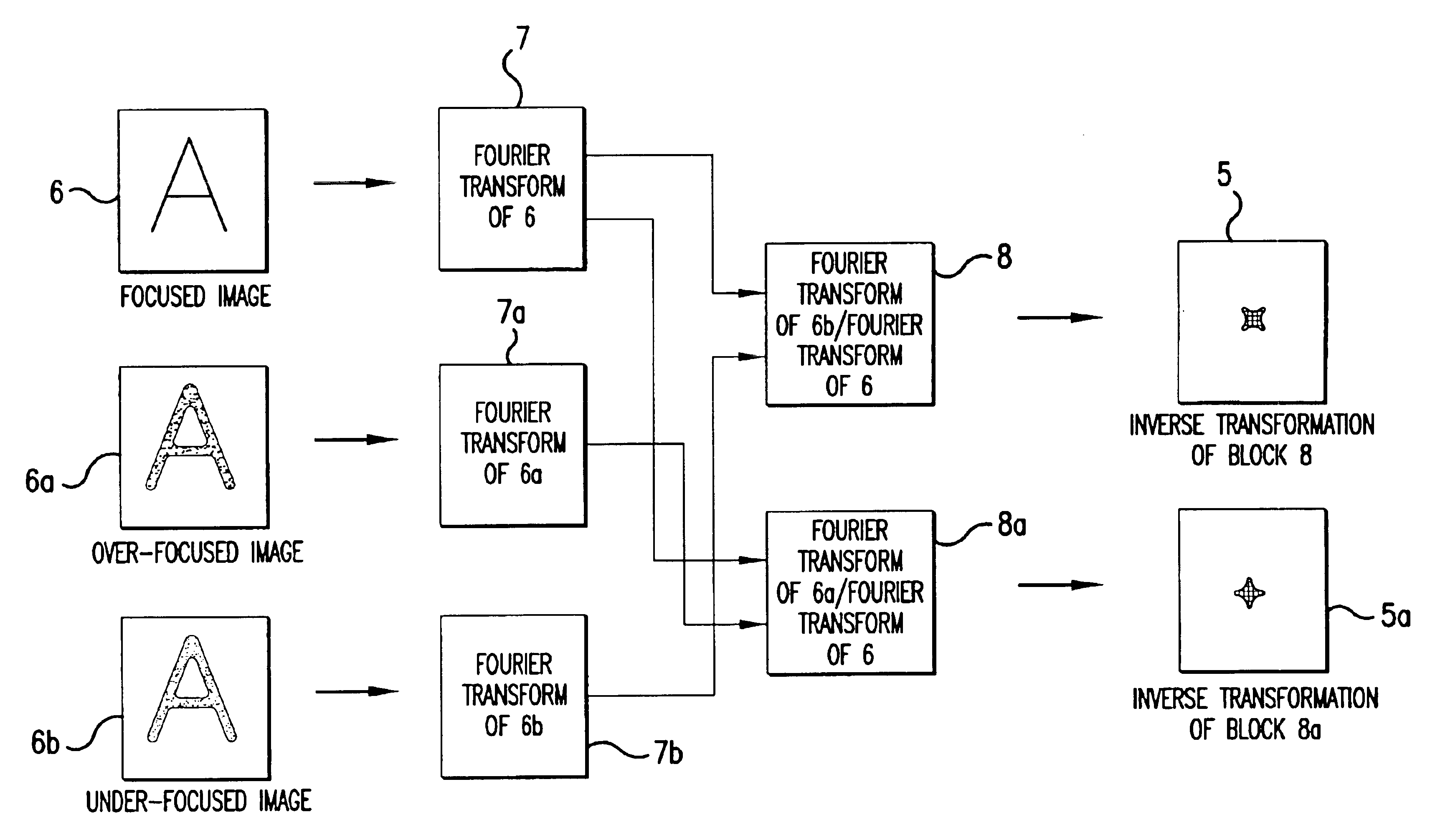
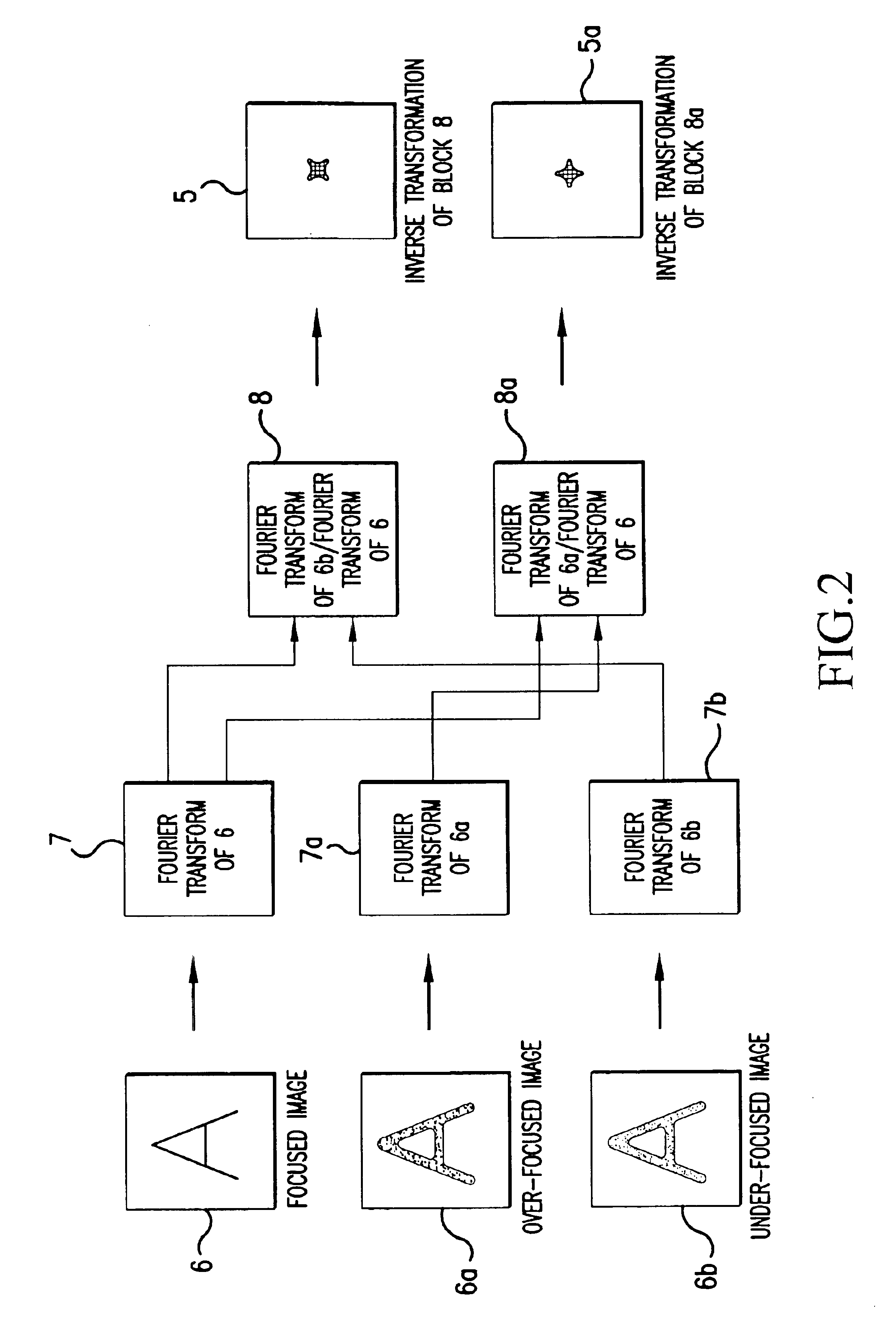
FIG. 2 shows the procedure by which the probe forms 5, 5a are obtained. To this end, the object 3 is imaged with a focussed, an overfocussed, and an underfocussed particle beam, and subsequently these images 6, 6a, 6b are subjected to a Fourier transformation. After division 8 of the transform 7a of the overfocussed image by the transform 7 of the focussed image, and the reverse transformation of the quotient, the information about ...
PUM
 Abstract
Description
Claims
Application Information


