Self-correcting I/O interface driver scheme for memory interface

a driver scheme and memory interface technology, applied in logic circuit coupling/interface arrangement, pulse technique, instruments, etc., can solve problems such as loss of gain timing margins, delay of i/o data path, path along,

a driver scheme and memory interface technology, applied in logic circuit coupling/interface arrangement, pulse technique, instruments, etc., can solve problems such as loss of gain timing margins, delay of i/o data path, path along,

US6859068B1Inactive Publication Date: 2005-02-22ORACLE INT CORP

Image

  • Self-correcting I/O interface driver scheme for memory interface
  • Self-correcting I/O interface driver scheme for memory interface
  • Self-correcting I/O interface driver scheme for memory interface

Examples


Embodiment Construction

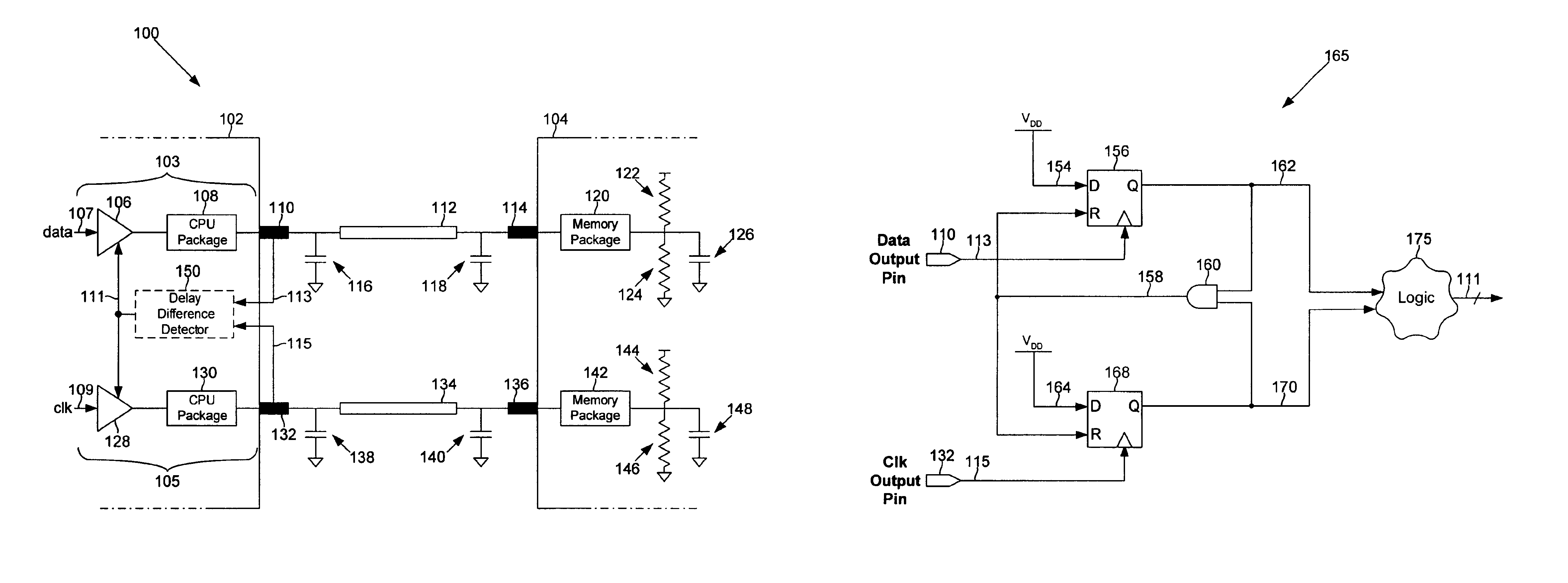
[0021]FIG. 4 shows an implementation of an I / O interface 51. Particularly, FIG. 4 shows an I / O interface of a microprocessor 53 and a memory circuit 54 (e.g., SRAM). Along an I / O data path 55 of the microprocessor 53, data 59 is driven by an I / O data driver 56 to a chip package 58, which, in turn, places the data 59 on data output pin 60. Data output pin 60 is used to “launch” the data 59 onto a printed circuit board (PCB) trace 62.

[0022]Data 59 launched onto the PCB trace 62 is received by the memory circuit 54 via a data input pin 64 of the memory circuit 54. In the memory circuit 54, the incoming data is propagated by a memory chip package 70 to termination resistors 72, 74.

[0023]Along an I / O clock path 57 of the microprocessor 53, a clock signal 61 is driven by an I / O clock driver 78 to a chip package 80, which, in turn, places the clock signal 61 on clock output pin 82. Clock output pin 82 is used to “launch” the clock signal 61 onto a PCB trace 84.

[0024]The clock signal 61 lau...


PUM


Abstract

A self-correcting I / O interface driver scheme uses a delay difference detector to detect a difference in delays between an I / O data path and an I / O clock path. The delay difference detector inputs signals from a data output pin connected to the I / O data path and a clock output pin connected to the I / O clock path. Upon determining a delay difference between the signals from the data and clock output pins, the delay difference detector generates signals to one or more drivers in the I / O data path and the I / O clock path. These signals from the delay difference detector are used to effectively adjust delays of the one or more drivers in order to effectively reduce the delay difference between the I / O data path and the I / O clock path.

Description

BACKGROUND OF INVENTION[0002]As shown in FIG. 1, a typical computer system 10 has, among other components, a microprocessor 12, one or more forms of memory 14, integrated circuits 16 having specific functionalities, and peripheral computer resources (not shown), e.g., monitor, keyboard, software programs, etc. These components communicate with one another via communication paths 18, e.g., wires, buses, etc., to accomplish the various tasks of the computer system 10.[0003]Communication between computer system components (e.g., from microprocessor 12 in FIG. 1 to integrated circuit 16 in FIG. 1) occurs across input / output (I / O) interfaces designed to facilitate the flow of data between computer system components. In one type of I / O interface, both a clock signal and data on a data signal are transmitted from a transmitting circuit to a receiving circuit. The receiving circuit uses the clock signal to latch the incoming data.[0004]Such I / O interfaces in which a clock signal of a transm...

Claims


Application Information

Patent Timeline
22 Feb 2005
Publication
US6859068B1
IPC
G11C7/10; H03K5/135; H03K19/003; H03L7/00; H03L7/081
CPC
G11C7/1051; G11C7/1066; G11C7/1078; G11C7/1093; H03K5/135; H03K19/00323; H03L7/00; H03L7/0812
Inventors
TRIVEDI, PRADEEP; ANANTHANARAYANAN, PRIYA