Semiconductor device and method for driving the same

a semiconductor and logic element technology, applied in semiconductor devices, digital storage, instruments, etc., can solve the problems of easy affecting total capacity, erased stored data, and above-mentioned conventional technologies, and achieve simplified semiconductor device structure, low power source voltage, and reliable threshold shift

Inactive Publication Date: 2005-02-22
PANASONIC CORP
View PDF14 Cites 7 Cited by
  • Summary
  • Abstract
  • Description
  • Claims
  • Application Information

AI Technical Summary

Benefits of technology

With this method, it is possible to write and read out information without using a negative voltage, so it is possible to lower the power source voltage and to simplify the structure of the semiconductor device.
In that ca...

Problems solved by technology

However, to store data, FFs include portions in which inverters are connected in series and to apply feedback, and moreover FFs are volatile, so that the stored data is erased when the power source is removed.
The above-mentioned conventional technologies, however, have encountered the following problems.
In MFISFETs, however, voltage is applied for creating polarization between the semiconductor substrate and the gate electrode, so depending on the structure of the semiconductor substrate, structural or operational problems may occur, such as a depletion layer becoming sandwiched between the portion of the semiconductor substrate to which voltage is applied and the gate electrode, or the total capacity being easily affected by the potential of the source region and the drain region.
This phenomenon is called read disturb, and when multiple read-outs are repeated, the ability to obtain the threshold shift necessary for a read-out ...

Method used


Image

  • Semiconductor device and method for driving the same
  • Semiconductor device and method for driving the same
  • Semiconductor device and method for driving the same

Examples


first embodiment

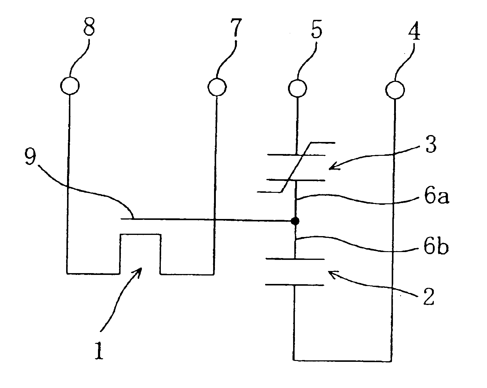
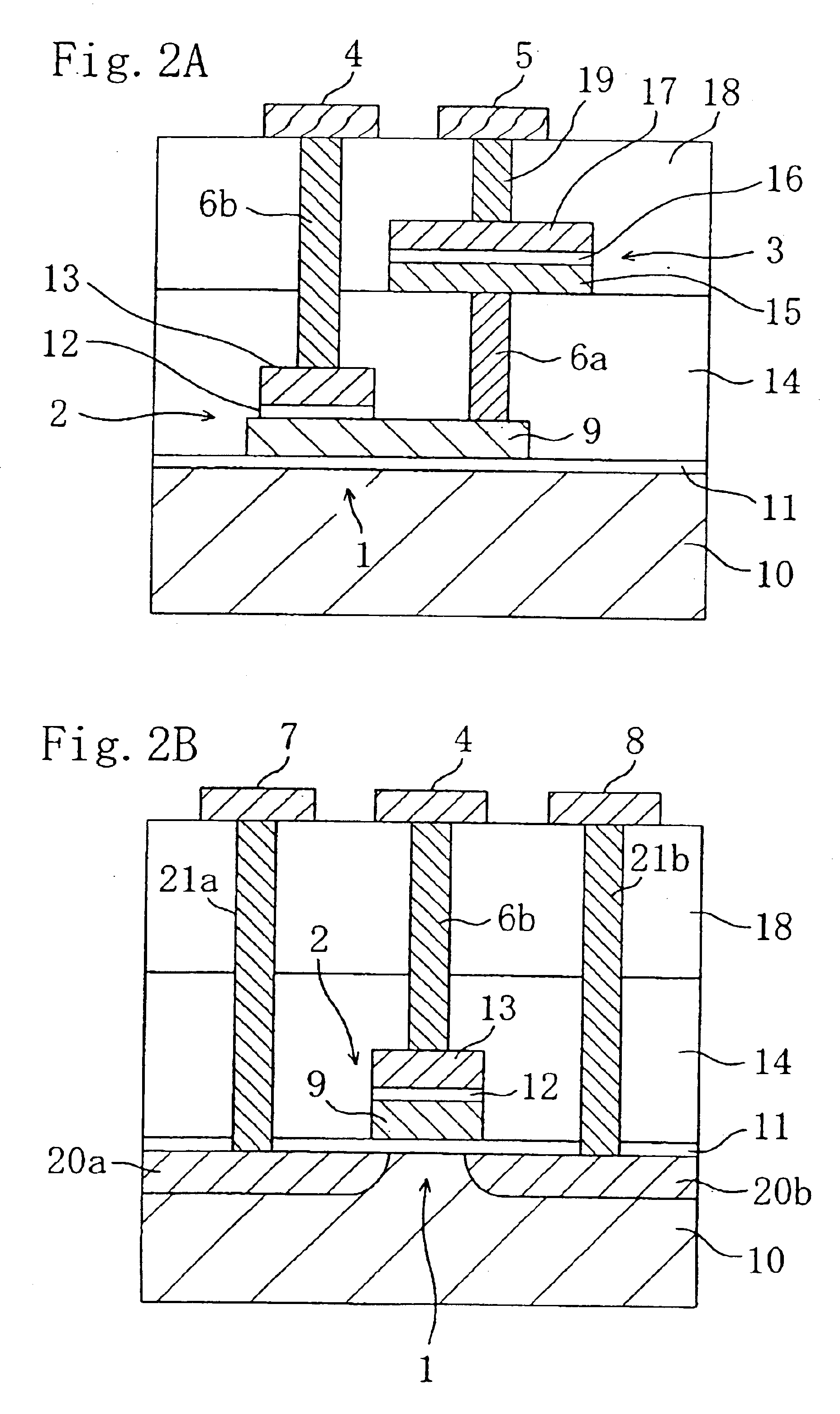
FIG. 1 is an equivalent circuit diagram of a nonvolatile semiconductor storage element (nonvolatile memory cell) according to the present invention.

As shown in FIG. 1, the nonvolatile semiconductor storage element of the present embodiment is provided with a MISFET 1, a floating gate electrode 9 of the MISFET 1, and a dielectric capacitor 2 and a ferroelectric capacitor 3, which are connected to the floating gate electrode 9 via a node 6a and a node 6b, respectively. Also, this nonvolatile semiconductor storage element is configured such that polarization can be generated as information in the ferroelectric film of the ferroelectric capacitor 3 by applying a voltage between a first polarization voltage supplying terminal 4 and a second polarization voltage supplying terminal 5. Furthermore, it is configured such that when read-out voltage is applied between a ground terminal 7 and a power source voltage terminal 8, which are connected to the source and drain regions of the MISFET 1,...

second embodiment

FIG. 4 is an equivalent electric circuit diagram of a nonvolatile semiconductor storage element (nonvolatile memory cell) according to a second embodiment of the present invention.

As shown in FIG. 4, in addition to the configuration of the semiconductor storage element according to the first embodiment, the nonvolatile semiconductor storage element of the present embodiment includes a pass transistor 25, which is provided between the MISFET 1 and the power source voltage terminal 8, and a control terminal 26, which is connected to the gate electrode of the pass transistor 25. In the present embodiment, structural components such as the MISFET 1, the dielectric capacitor 2, the ferroelectric capacitor 3, the first polarization voltage application terminal 4, the second polarization voltage application terminal 5, the ground terminal 7, and the power source voltage terminal 8, are the same as those of the first embodiment, so further diagrammatic illustration and description of the st...

third embodiment

FIG. 5 is an equivalent circuit diagram of a nonvolatile semiconductor storage element according to a third embodiment of the present invention.

As shown in FIG. 5, the nonvolatile semiconductor storage element of the present embodiment includes, in addition to the structure of the semiconductor storage element according to the first embodiment, a control gate electrode 27, which is provided above the floating gate electrode 9 of the MISFET 1 and sandwiches the insulating film therewith, and a control voltage applying terminal 28 for applying a read-out voltage to the control gate electrode 27. That is to say, in addition to the MISFET 1, the dielectric capacitor 2, the ferroelectric capacitor 3, the first polarization voltage application terminal 4, the second polarization voltage application terminal 5, the ground terminal 7, and the power source voltage terminal 8 of the nonvolatile semiconductor storage element of the first embodiment as shown in FIGS. 2A and 2B, the nonvolatile ...


PUM


Abstract

A nonvolatile semiconductor storage element, which is provided with a floating gate electrode, and a dielectric capacitor and a ferroelectric capacitor both connected to the floating gate electrode. By applying voltage between a first polarization voltage supplying terminal and a second polarization voltage supplying terminal, polarization serving as information is generated in the ferroelectric film of the ferroelectric capacitor. Additionally, when a read-out voltage is applied between the ground terminal and the power source voltage terminal that are in connection with the source and drain regions, the MISFET is turned either on or off in correspondence to the state of the charge held in the floating gate electrode, and thus information within the floating gate electrode is read out.

Description

BACKGROUND OF THE INVENTIONThe present invention relates to a nonvolatile memory cell and a logic element device that use a ferroelectric layer.Nonvolatile memories have become indispensable devices in conjunction with the recent miniaturization of devices and advances in portable devices. Flash memories and ferroelectric memories (FRAM) are nonvolatile memories that have already made their way into the market. In particular, miniaturized nonvolatile memories capable of high-speed operation have been proposed that use ferroelectrics for a portion of the insulating film, such as the gate insulating film, of a MISFET (metal insulator semiconductor field effect transistor). MISFETs using such a ferroelectric layer include MFISFETs using electrodes (M), ferroelectric layers (F), insulating layers (I) made from a regular dielectric material and Si substrates (S), and MFMISFETs using upper electrodes (M), ferroelectrics (F), middle electrodes (M), and gate insulating films (I) made of a r...

Claims


Application Information

Patent Timeline
IPC IPC(8): G11C11/22H01L29/66H01L27/115H01L29/423H01L29/40H01L29/788G11C16/04H01L21/8246
CPCG11C11/22H01L29/7881H01L27/11507H01L29/42324H01L27/11502G11C16/0408H10B53/30H10B53/00
Inventor OHTSUKA, TAKASHIMORITA, KIYOYUKIUEDA, MICHIHITO
Owner PANASONIC CORP
Why Eureka
Try Eureka