NAND type flash EEPROM in which sequential programming process is performed by using different intermediate voltages

a technology of sequential programming and intermediate voltage, which is applied in the field of nand-type flash eeprom data programming system, can solve the problems of scaling and increasing the erroneous programming stress, and the programming stress decreases

Inactive Publication Date: 2005-02-22
KIOXIA CORP
View PDF6 Cites 109 Cited by
  • Summary
  • Abstract
  • Description
  • Claims
  • Application Information

AI Technical Summary

Problems solved by technology

However, the Vpass stress characteristic is the same as that in the SB system, but it is considered that the Vpgm stress becomes smaller than that in the SB system, and therefore, the intersection is shifted down to the left (erroneous programming stress decreases).
As the result of this, the scaling tends to increase the erroneous programming stress.
However, if the multi-value storage system is used, the threshold voltage range of the memory transistor used for data recording is enlarged, and therefore, it is inevitably necessary to enhance the program voltage Vpgm.

Method used


Image

  • NAND type flash EEPROM in which sequential programming process is performed by using different intermediate voltages
  • NAND type flash EEPROM in which sequential programming process is performed by using different intermediate voltages
  • NAND type flash EEPROM in which sequential programming process is performed by using different intermediate voltages

Examples


first embodiment

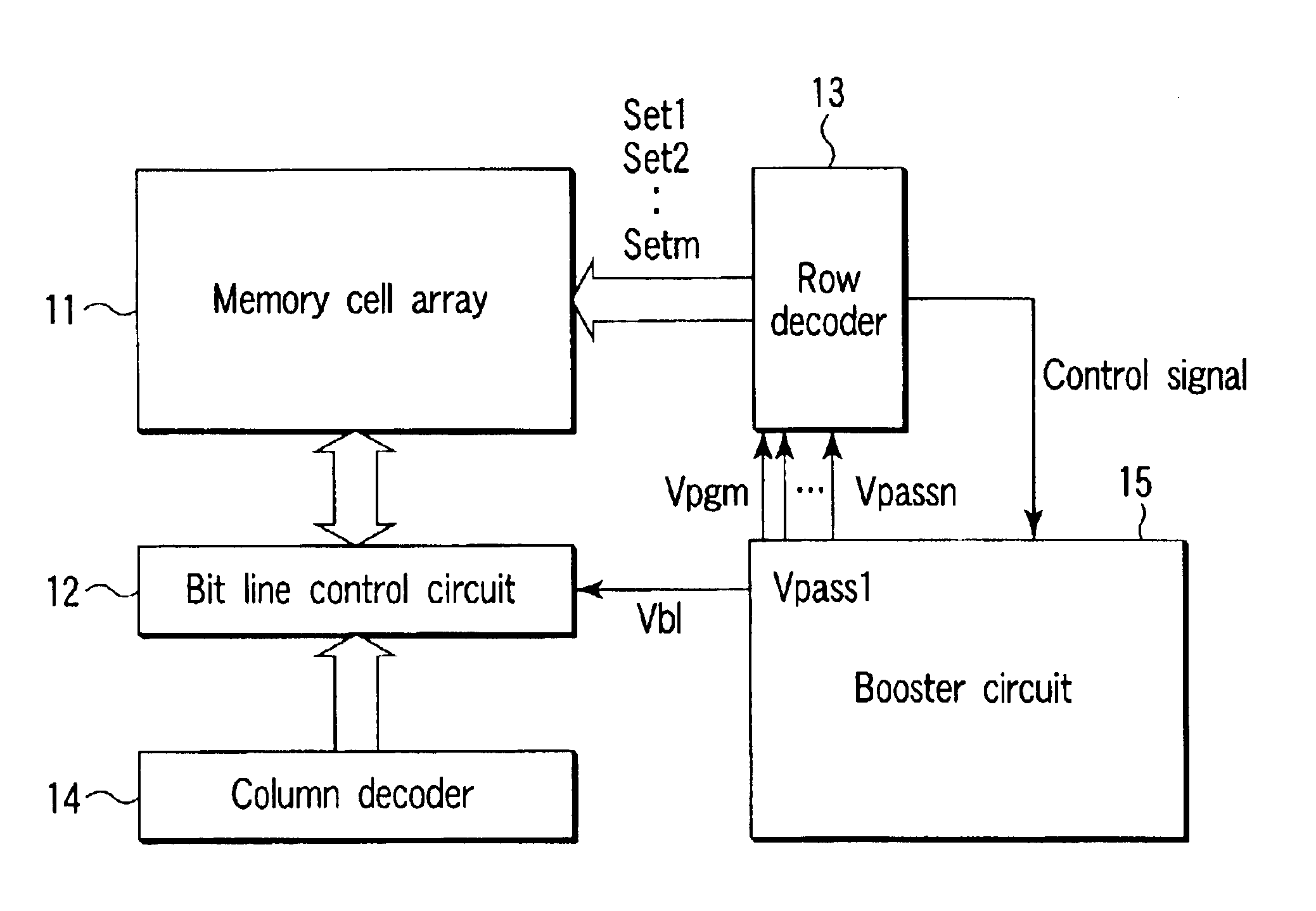
FIG. 5 is a block diagram showing an extracted main portion of a nonvolatile semiconductor memory device according to a first embodiment of the present invention, for illustrating the nonvolatile semiconductor memory device. In a memory cell array 11, NAND cell units are arranged in row and column directions in a matrix form, and control gate lines, bit lines, selection gate lines, source lines and the like are wired. A bit line control circuit 12 and row decoder 13 are connected to the memory cell array 11. The bit line control circuit 12 performs operations of latching program data, sensing data at the readout time and the like. A column decoder 14 which decodes a column address signal to select a column of the NAND cell units is connected to the bit line control circuit 12. A booster circuit 15 creates and generates program voltage Vpgm, a plurality of different intermediate voltages Vpass1 to Vpassn and bit line voltage Vbl from the power supply voltage. The row decoder 13 suppl...

second embodiment

A nonvolatile semiconductor memory device according to a second embodiment of this invention has basically the same configuration as that of the first embodiment and can be realized by modifying the row decoder 13 in the circuit of FIG. 5 to perform the selection operation as will be described below.

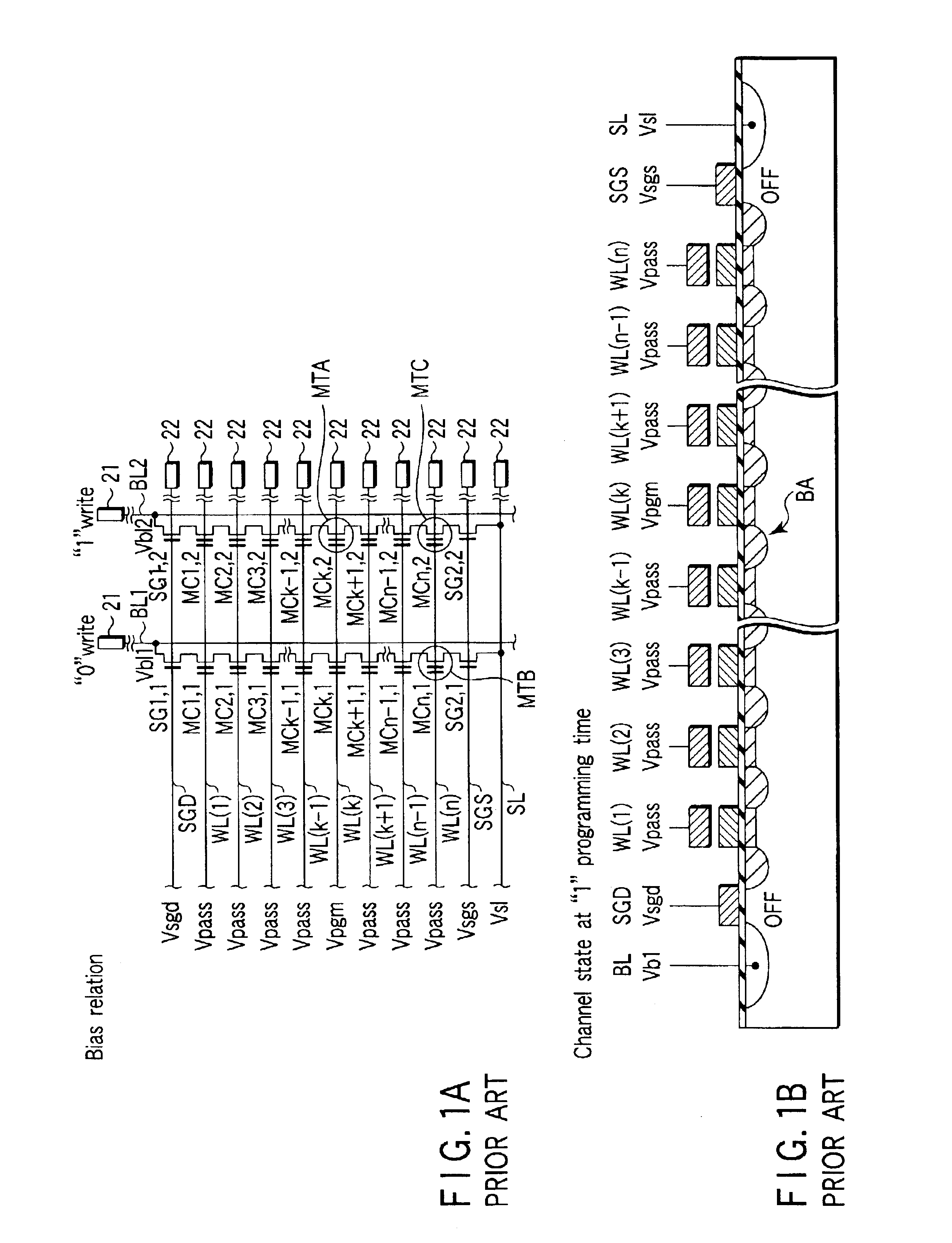
FIGS. 9A, 9B and 9C are equivalent circuit diagrams showing bias states at the time of data programming into memory transistors respectively connected to the nth, kth and first control gate lines from the bit line side. In the present embodiment, it is assumed that the programming process is a sequential programming process performed in order from the control gate line WL(n) on the source side to the control gate line WL(1) on the bit line side. Program voltage Vpgm is applied to a selected control gate line WL(k). Low voltage Vcutoff (for example, 0V) which cuts off the memory transistor is applied to the control gate line WL(k+1) which lies adjacent to and on the source line side of th...

third embodiment

A nonvolatile semiconductor memory device according to a third embodiment of this invention has basically the same configuration as that of the first embodiment and can be realized by modifying the row decoder 13 in the circuit of FIG. 5 to perform the selection operation as will be described below.

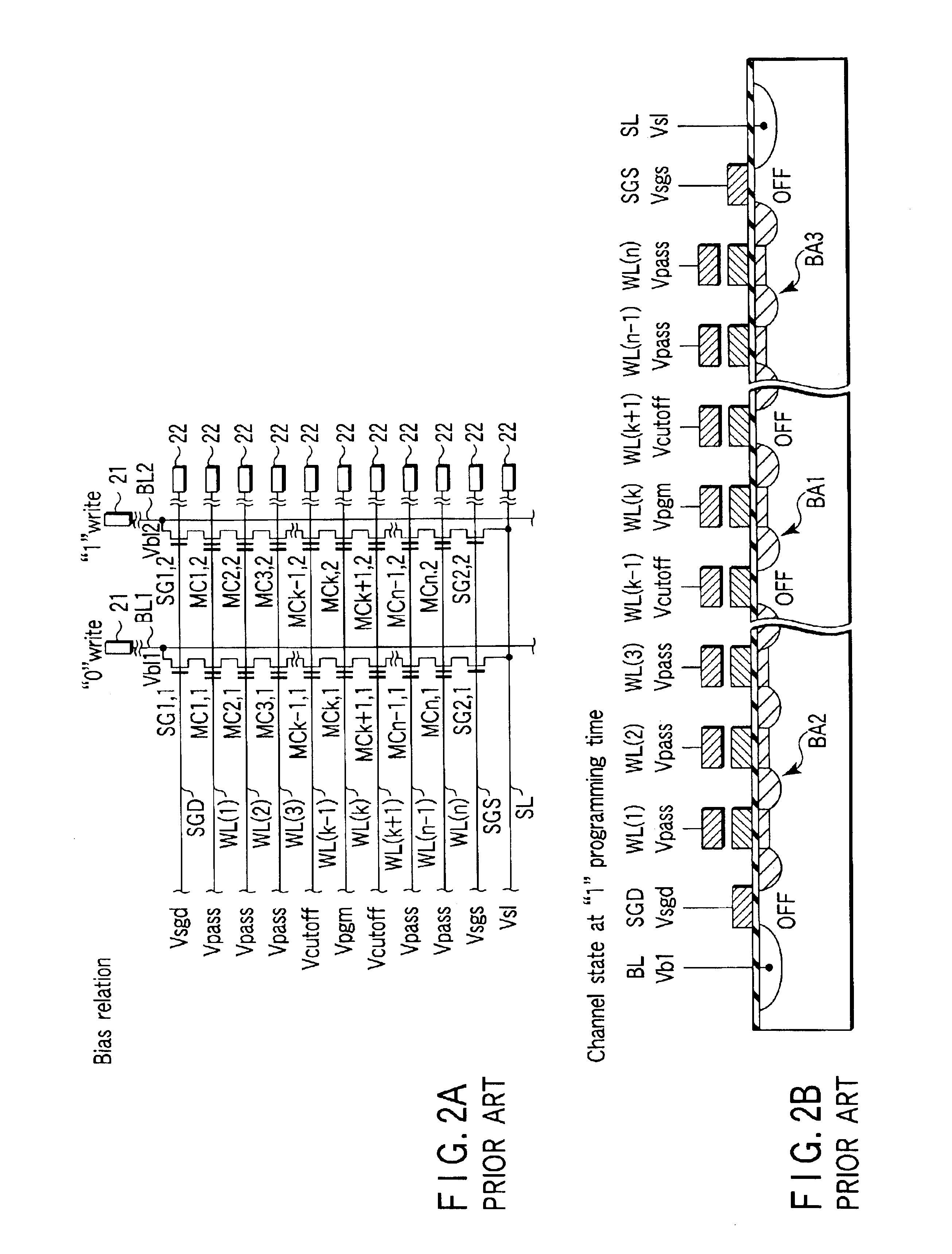
FIGS. 10A, 10B and 10C are equivalent circuit diagrams showing bias states at the time of data programming into memory transistors respectively connected to the nth, kth and first control gate lines from the bit line side. In the present embodiment, it is assumed that the programming process is a sequential programming process performed in order from a control gate line WL(n) on the source side to a control gate line WL(1) on the bit line side. Program voltage Vpgm is applied to a selected control gate line WL(k). Low voltage Vcutoff (for example, 0V) which cuts off the memory transistor is applied to a control gate line WL(k+j) (j is an integer equal to or larger than 2). Intermediate vo...


PUM


Abstract

A nonvolatile semiconductor memory device includes a NAND memory cell array, booster circuit, row decoder, bit line control circuit and column decoder. In the device, the magnitude of intermediate voltage applied to the control gates of memory transistors from the booster circuit via the row decoder is changed according to the position of a selected control gate line when data is sequentially programmed into the memory transistors in the memory cell array. Alternatively, a plurality of different intermediate voltages are applied when data is simultaneously programmed into memory transistors connected to the selected control gate line.

Description

CROSS-REFERENCE TO RELATED APPLICATIONSThis application is based upon and claims the benefit of priority from the prior Japanese Patent Application No. 2002-349199, filed Nov. 29, 2002, the entire contents of which are incorporated herein by reference.BACKGROUND OF THE INVENTION1. Field of the InventionThis invention relates to a nonvolatile semiconductor memory device, and more specifically, to a data programming system of a NAND type flash EEPROM, for example.2. Description of the Related ArtAs a nonvolatile semiconductor memory device which can be electrically rewritten and formed with high integration density, a NAND type flash EEPROM is well known in the art. A memory transistor in the NAND type flash EEPROM has a stacked gate structure in which a charge storage layer (floating gate) and control gate are stacked and formed above a semiconductor substrate with an insulating film disposed therebetween. A NAND cell unit is configured by serially connecting a plurality of memory tr...

Claims


Application Information

Patent Timeline
Patent Type & Authority Patents(United States)
IPC IPC(8): G11C16/04G11C16/10G11C16/06G11C16/02H01L27/115
CPCG11C16/0483G11C16/10H10B69/00
Inventor MATSUNAGA, YASUHIKOYAEGASHI, TOSHITAKEARAI, FUMITAKA
Owner KIOXIA CORP
Why Eureka
Try Eureka