Laser modulator

a laser modulator and light signal technology, applied in the direction of laser details, semiconductor lasers, electrical apparatus, etc., can solve the problems of increasing the severity of dispersion problems, shifting the wavelength of primary flight signals, and reducing the efficiency of lasers, so as to achieve high efficiency and flexibility, reduce the effect of power consumption and small siz

Inactive Publication Date: 2005-02-22
II VI DELAWARE INC
View PDF9 Cites 5 Cited by
  • Summary
  • Abstract
  • Description
  • Claims
  • Application Information

AI Technical Summary

Benefits of technology

The object of the present invention is therefore to provide a solution for the production of information carrying (i.e. modulated) light signals, which alleviates the problems above and thus offers a power and size efficient design of moderate circuit complexity.
The invention offers a highly efficient and flexible solution for generating modulated light signals. Simultaneously, the invention vouches for power efficient designs of comparatively small sizes and moderate circuit complexity. Naturally, the invention will therefore provide a competitive edge to any communication system where optical transmitters are utilized for the transmission of information.

Problems solved by technology

A direct modulated laser, however, inevitably shifts the wavelength of the primary flight signal to some degree when the signal is modulated.
This causes dispersion, i.e. degradation of the signal due to the fact that the various wave components experience different propagation velocities.
The severity of the dispersion problem increases with increased bitrate and fiber length.
The laser here operates at a constant current, which results in a relatively low chirp (i.e. undesired rapid changing of the frequency / wavelength).
However, the design is comparatively bulky and expensive.
This in turn, gives rise to a comparatively large, complex and expensive circuitry.
Typically, the required voltage swing is higher than what can be accomplished by means of a high-speed CMOS process (CMOS=complementary metal-oxide semiconductor), which of course, places severe restrictions and demands on the modulator driver.

Method used


Image

  • Laser modulator
  • Laser modulator
  • Laser modulator

Examples


first embodiment

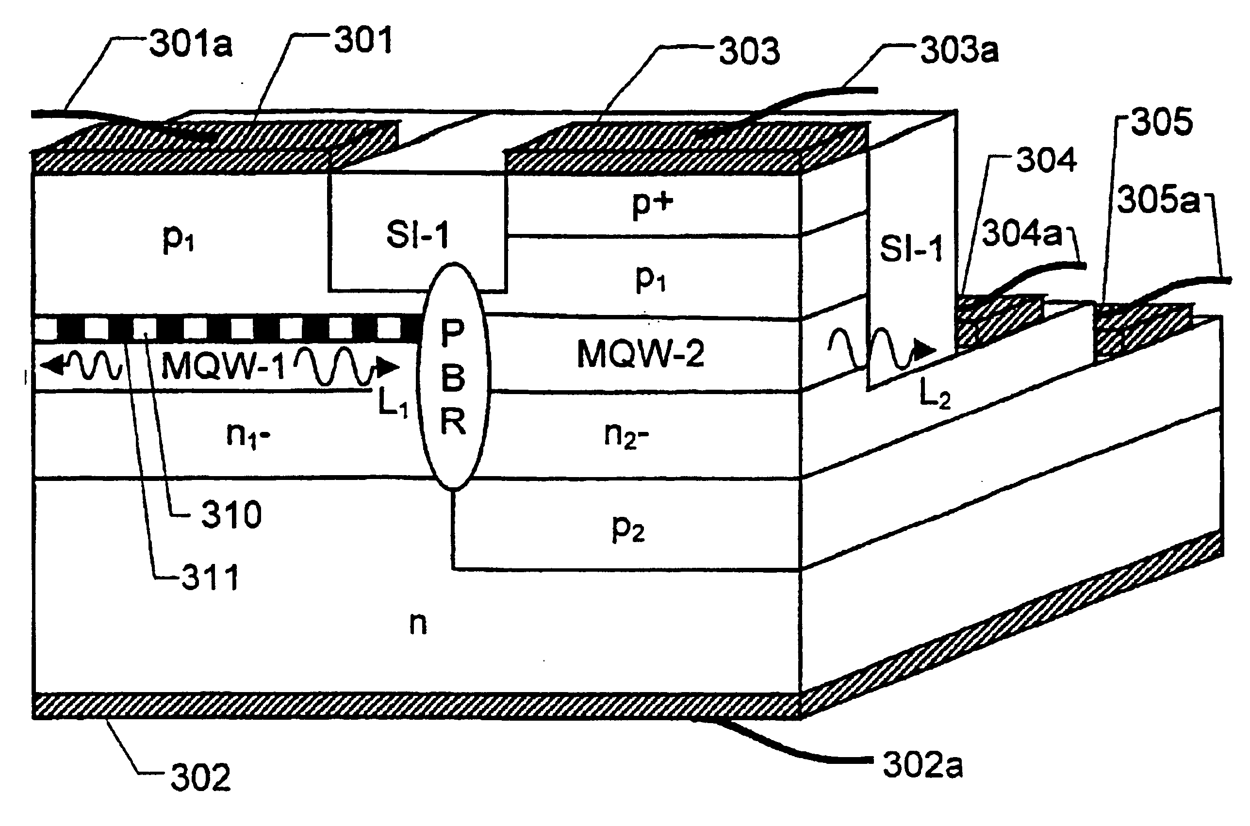
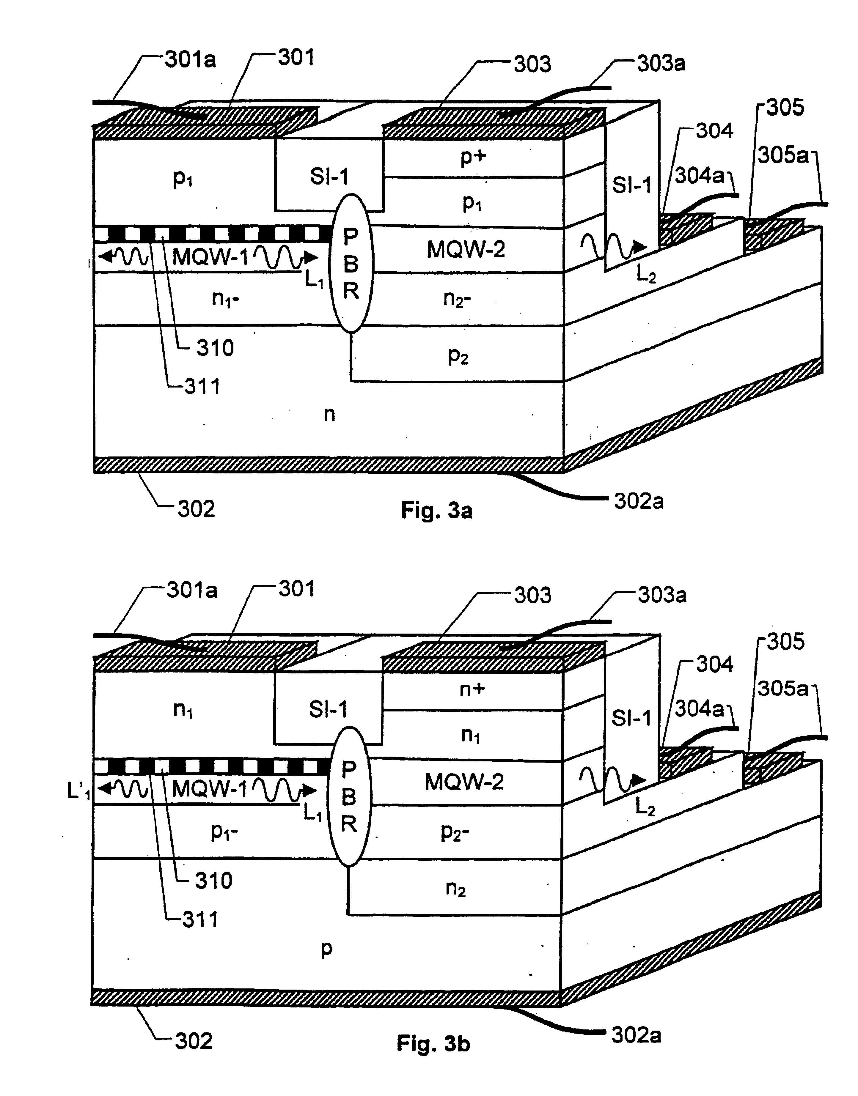
FIG. 3a shows an integrated laser-modulator structure according to a first alternative of the invention. A laser section here contains a separate anode area of a positive doping polarity p1 (e.g. InP), which is accessible via a first anode contact 301 and a first anode lead 301a. Correspondingly, the modulator section contains another separate anode area p+ (e.g. InGaAs), also of positive doping polarity, which is accessible via a second anode contact 303 and a second anode lead 303a. A semi-insulating region (i.e. un-doped area) SI-1 (e.g. InP) separates the laser anode area p1 from the modulator anode area p+. A sub-layer p1 of the anode area p+ in the modulator section 252, extends below the first un-doped area SI-1 and contacts the laser anode area pi.

The laser section has a two-layered cathode area containing a first layer n1− (e.g. InP) of negative doping polarity and a substrate n (e.g. InP), also of negative doping polarity. The modulator section has a corresponding cathode ...

second embodiment

FIG. 5b shows a block diagram over a proposed optical transmitter, which includes a laser unit 450 according to the invention. This embodiment is especially adapted for producing a relatively low-frequency outgoing modulated light signal L2 (i.e. with a comparatively low lower cut-off frequency). All units and components bearing the same identifiers as used in FIG. 5a here have the same functions as described above with reference to this figure. However, a second resistor 423 and a second capacitor 424 are added in order to provide a sufficient termination of the higher frequencies. For the same reason, a third capacitor 428 has been added between the second resistor 427 and the ground potential. Furthermore, both the second capacitor 424 and the third capacitor 428 are connected to the modulator driver 420. The extra capacitors 424 and 428 are necessary because there is a physical limit as to the highest possible value for the first capacitor 422 (and as a consequence thereof a low...


PUM


Abstract

An integrated device is provided having both laser and modulator sections. The laser section generates a primary light signal using a distributed feedback process. The modulator section influences the primary light signal by means of an electroabsorption process. The laser and modulator sections are electrically separated from each other with respect to anode and cathode areas. As a result, a single supply voltage can be used to operate the device. An optical transmitter contains, in addition to the integrated device, a protocol converter which receives an information signal to be transmitted and generates a control signal which is received by a modulator driver. Based thereon, the modulator driver produces a modulating signal, which causes a modulated light signal representing the information signal to be output. A laser bias control unit controls the output power level of the primary light signal based on a leak signal from the laser section.

Description

FIELD OF THE INVENTIONThe present invention relates generally to the production of modulated light signals for transmission of information. More particularly the invention relates to an integrated device for emitting a modulated light signal according to the preamble of claim 1 and an optical transmitter according to the preamble of claim 10.THE BACKGROUND OF THE INVENTION AND PRIOR ARTOptical communication systems transport information in the form of modulated fight signals. A semiconductor laser is normally used to accomplish these signals (laser=light amplification by stimulated emission of radiation). A direct modulated laser, however, inevitably shifts the wavelength of the primary flight signal to some degree when the signal is modulated. This causes dispersion, i.e. degradation of the signal due to the fact that the various wave components experience different propagation velocities. The severity of the dispersion problem increases with increased bitrate and fiber length. Tod...

Claims


Application Information

Patent Timeline
Patent Type & Authority Patents(United States)
IPC IPC(8): H01S5/00H01S5/026H01S5/042
CPCH01S5/0265H01S5/0425H01S5/042H01S5/04256
Inventor SVENSON, LARS-GOTE
Owner II VI DELAWARE INC
Why Eureka
Try Eureka