Bilayer microstrip reflector antenna

a microstrip reflector and antenna technology, applied in the field of antennas, can solve the problems of narrow gain-bandwidth and reduce the efficiency of antennas, and achieve the effects of reducing radiation level, improving antenna gain-bandwidth, and eliminating interferen

Inactive Publication Date: 2005-03-01
TATUNG UNIVERSITY +1
View PDF2 Cites 4 Cited by
  • Summary
  • Abstract
  • Description
  • Claims
  • Application Information

AI Technical Summary

Benefits of technology

It is the main object of the present invention to provide a bilayer microstrip reflector antenna, which greatly improves antenna gain-bandwidth, eliminate interferences between antennas, and reducing radiation level from phase-delay circuit.
To achieve this and other objects of the present invention, the bilayer microstrip reflector antenna comprises a bilayer printed circuit board used with a horn antenna. The bilayer printed circuit board comprises a first dielectric layer and a second dielectric layer abutted against the first dielectric layer. The first dielectric layer has a thickness, a dielectric constant, a plurality of antenna units disposed on one face, and a plurality of phase-delay circuit units disposed on the other face respectively corresponding to the antenna units, wherein the phase-delay circuit units each overlapping the corresponding antenna unit a distance. The second dielectric layer has a thickness and a dielectric constant. Therefore, a better gain-bandwidth can be obtained by means of adjusting the overlapping distance of the antenna units and the phase-delay circuit units, side length of the antenna units and the dielectric constant and thickness of the two dielectric layers. Surface wave phenomenon can be reduced by means of selecting a relatively lower dielectric constant. A satisfactory grounding effect can be obtained to reduce radiation from phase-delay circuit units by lowering the second dielectric layer toward the ground.

Problems solved by technology

However, conventional microstrip reflector antennas that achieve concentration of antenna beam by different methods have the common problem of narrow gain-bandwidth.
Increasing the thickness of the dielectric layer may cause the so-called surface wave phenomenon, thereby reducing antenna efficiency accompanying with the problem of high radiation level from delay circuit.

Method used


Image

  • Bilayer microstrip reflector antenna
  • Bilayer microstrip reflector antenna
  • Bilayer microstrip reflector antenna

Examples


Embodiment Construction

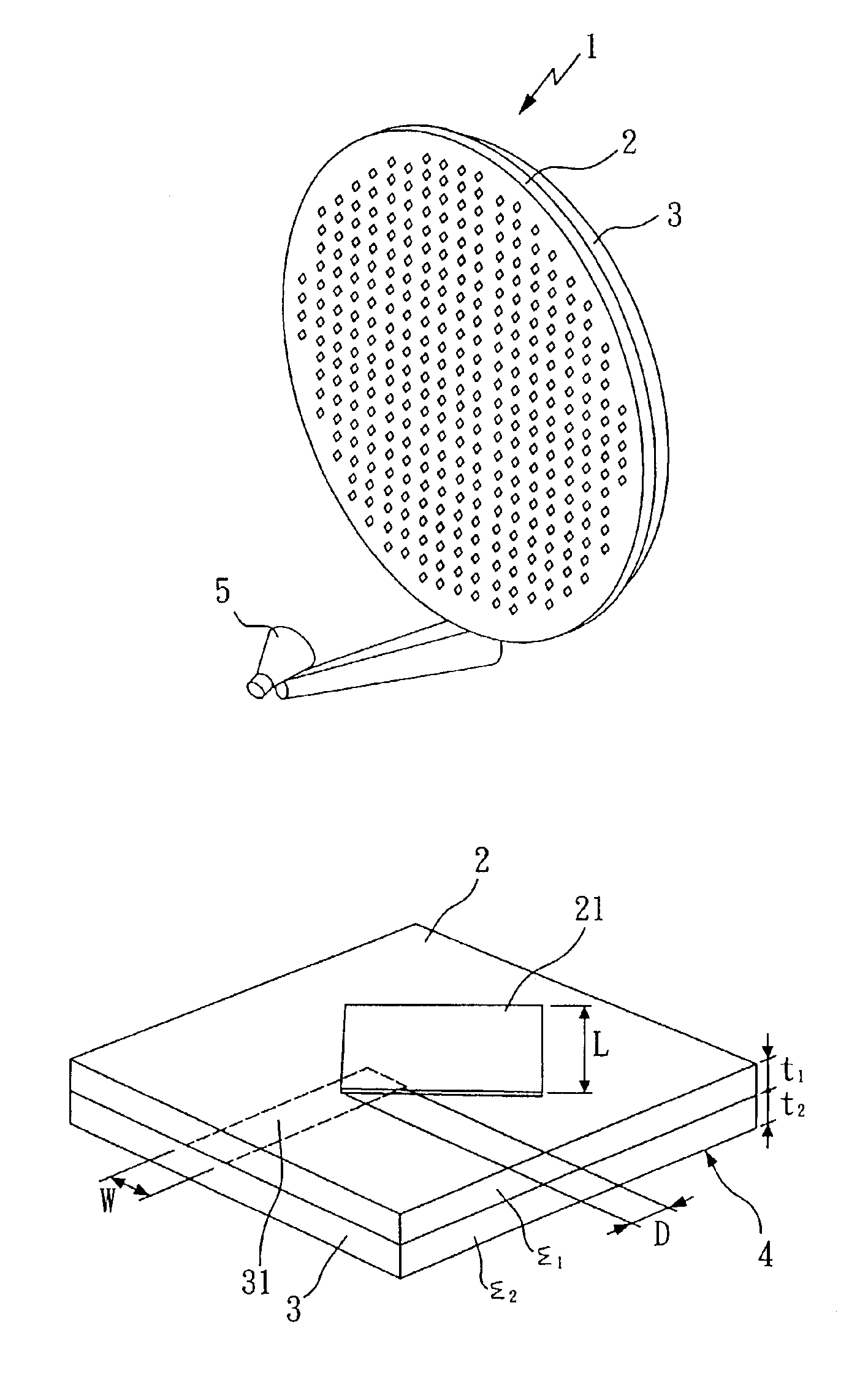
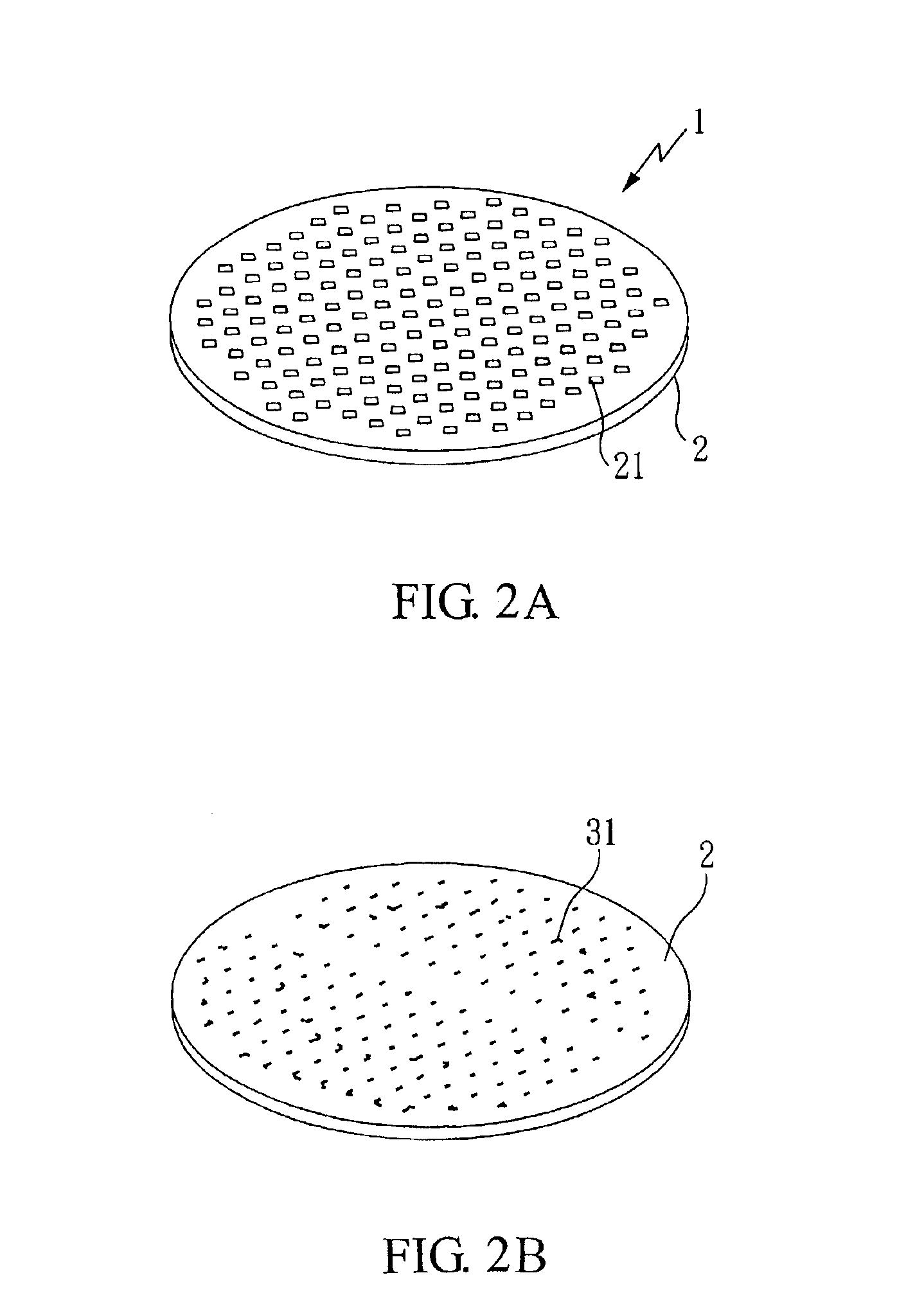
Referring to FIG. 1, a circular bilayer microstrip reflector antenna 1 is shown comprised of a first dielectric layer 2, a second dielectric layer 3 abutting against the first dielectric layer 2, and a horn antenna 5. As illustrated in FIGS. 2a and 2b, the aforesaid first dielectric layer 2 comprises a plurality of antenna units 21 on one face and a plurality of phase-delay circuit units 31 on the other face. The phase-delay circuit units 31 are sandwiched between the first dielectric layer 2 and the second dielectric layer 3. Referring to FIG. 3, the first dielectric layer 2 has a thickness t1 and a dielectric constant ε1. The second dielectric layer 3 that abuts to the first electric layer 2, has a thickness t2 and a dielectric constant ε2. According to this embodiment, the antenna units 21 in the first dielectric layer 2 are rhombic, having a side length L; the phase-delay circuit units 31 are rectangular, having a width W. The phase-delay circuit units 31 each overlapping the co...


PUM


Abstract

A bilayer microstrip reflector antenna is disclosed to include a first dielectric layer, the first dielectric layer having antenna units and phase-delay circuit units overlapped on antenna units, and a second dielectric layer abutting against the first dielectric layer. A better gain-bandwidth is obtained by adjusting the overlapping distance of the antenna units and phase-delay circuit units, side length of antenna units and the dielectric constant and thickness of the two dielectric layers. Surface wave phenomenon is reduced by means of selecting a relatively lower dielectric constant. A satisfactory grounding effect is obtained to reduce radiation from phase-delay circuit units by lowering the second dielectric layer toward the ground.

Description

BACKGROUND OF THE INVENTION1. Field of the InventionThe present invention relates to antennas and, more particularly, to a planar bilayer microstrip reflector antenna that increases the antenna gain-bandwidth.2. Description of Related ArtIn comparison with parabolic reflector antennas, micros trip reflector antennas employ relatively new technology. A parabolic reflector antenna has a curved surface. A microstrip reflector antenna can be made having a planar surface. Further, a microstrip reflector antenna can achieve the concentration of antenna beam in a particular direction by means of the application of one of several methods.However, conventional microstrip reflector antennas that achieve concentration of antenna beam by different methods have the common problem of narrow gain-bandwidth. Methods of improving the problem of narrow gain-bandwidth are reported in specific issues. However, these reports are commonly of a single layer design formed of a single printed circuit board ...

Claims


Application Information

Patent Timeline
Patent Type & Authority Patents(United States)
IPC IPC(8): H01Q3/46H01Q19/13H01Q19/10H01Q19/195H01Q3/00
CPCH01Q3/46H01Q19/195H01Q19/132
Inventor CHANG, THE-NANWEI, YU-CHENG
Owner TATUNG UNIVERSITY
Why Eureka
Try Eureka