
Method of production of a patterned semiconductor layer

a technology of patterned semiconductor layer and manufacturing method, which is applied in the direction of semiconductor lasers, laser details, electrical apparatus, etc., can solve the problems of natural oxide of silicon, siosub>2/sub>, and substrate exposure to uncontrolled contamination, and achieve maximum replicable component characteristics and reasonable engineering effort and expense

Inactive Publication Date: 2005-03-08
OSRAM OPTO SEMICON GMBH & CO OHG
View PDF18 Cites 1 Cited by
  • Summary
  • Abstract
  • Description
  • Claims
  • Application Information

AI Technical Summary

Benefits of technology

The present invention provides a method for producing semiconductor components that avoids the need for removing the semiconductor substrate from the epitaxy reactor and high temperature steps. The method involves applying a masking layer on the substrate, growing semiconductor layers in the masking layer, and then removing the masking layer through use of an etchant. The invention also provides a method for producing laterally integrated semiconductor components by applying semiconductor components on an epitaxial substrate and layering masking layers on the substrate and components. The use of HF soluble masking layers allows for the application of different materials without interrupting the process as a whole, reducing the need for later lithographic processes and cost savings. The invention also allows for the selective removal of areas intended for optoelectronic semiconductor components while protecting the electrical components with a thinner layer of HF soluble masking material.

Problems solved by technology

The natural oxide of the silicon, SiO2, which is created by the contact of the substrate with oxygen, produces considerable problems.
Accordingly, the substrate may be exposed to uncontrolled contamination.
By multiple insertions and removals of the substrate into and from the reactor, the above processes become susceptible to faults, the gain of functional components decreases, and the production costs increase.
During the high temperature step of removing the natural oxide of the silicon, at least the electrical components may be damaged.

Method used


Image

  • Method of production of a patterned semiconductor layer
  • Method of production of a patterned semiconductor layer
  • Method of production of a patterned semiconductor layer

Examples


Embodiment Construction

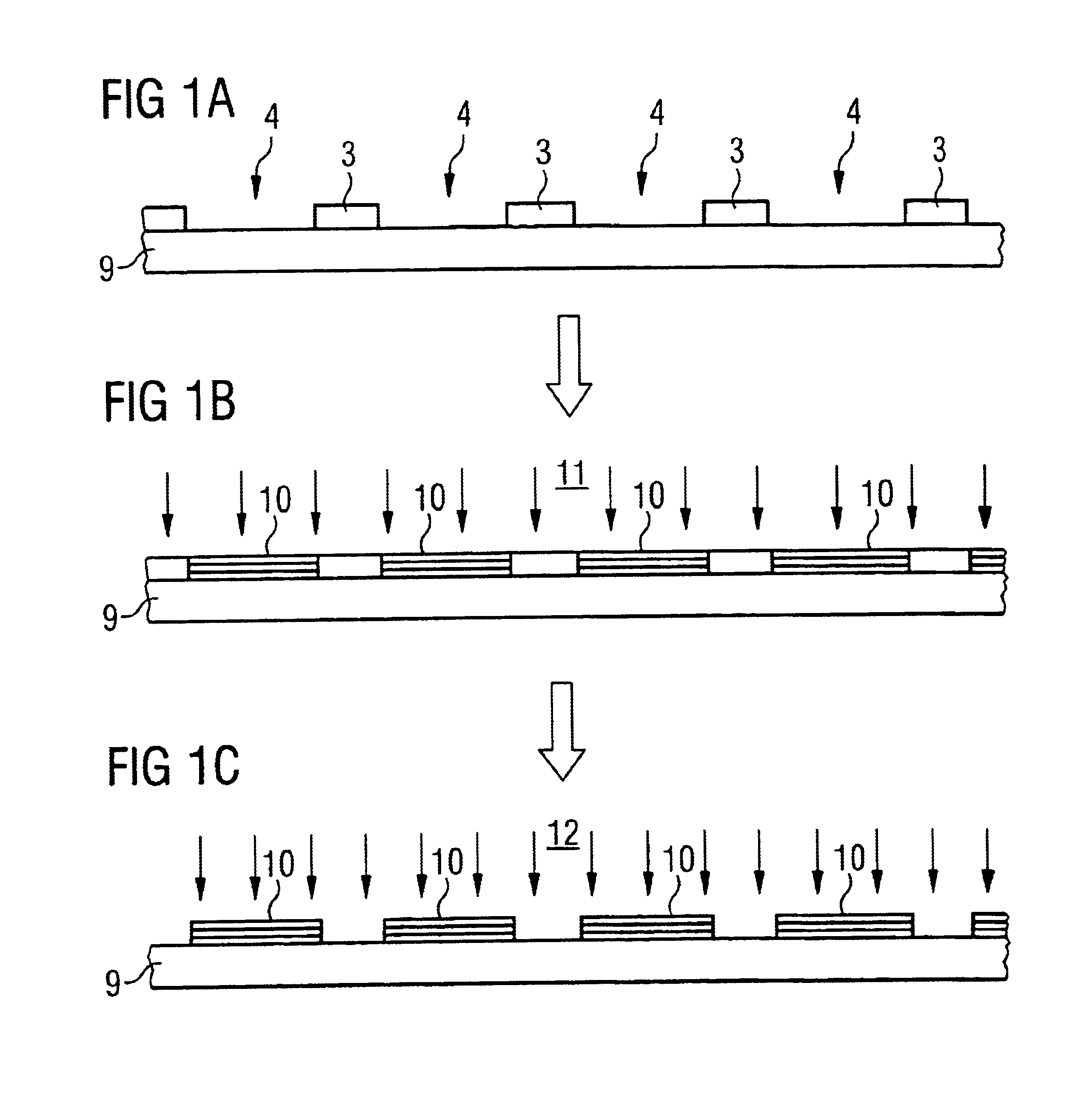
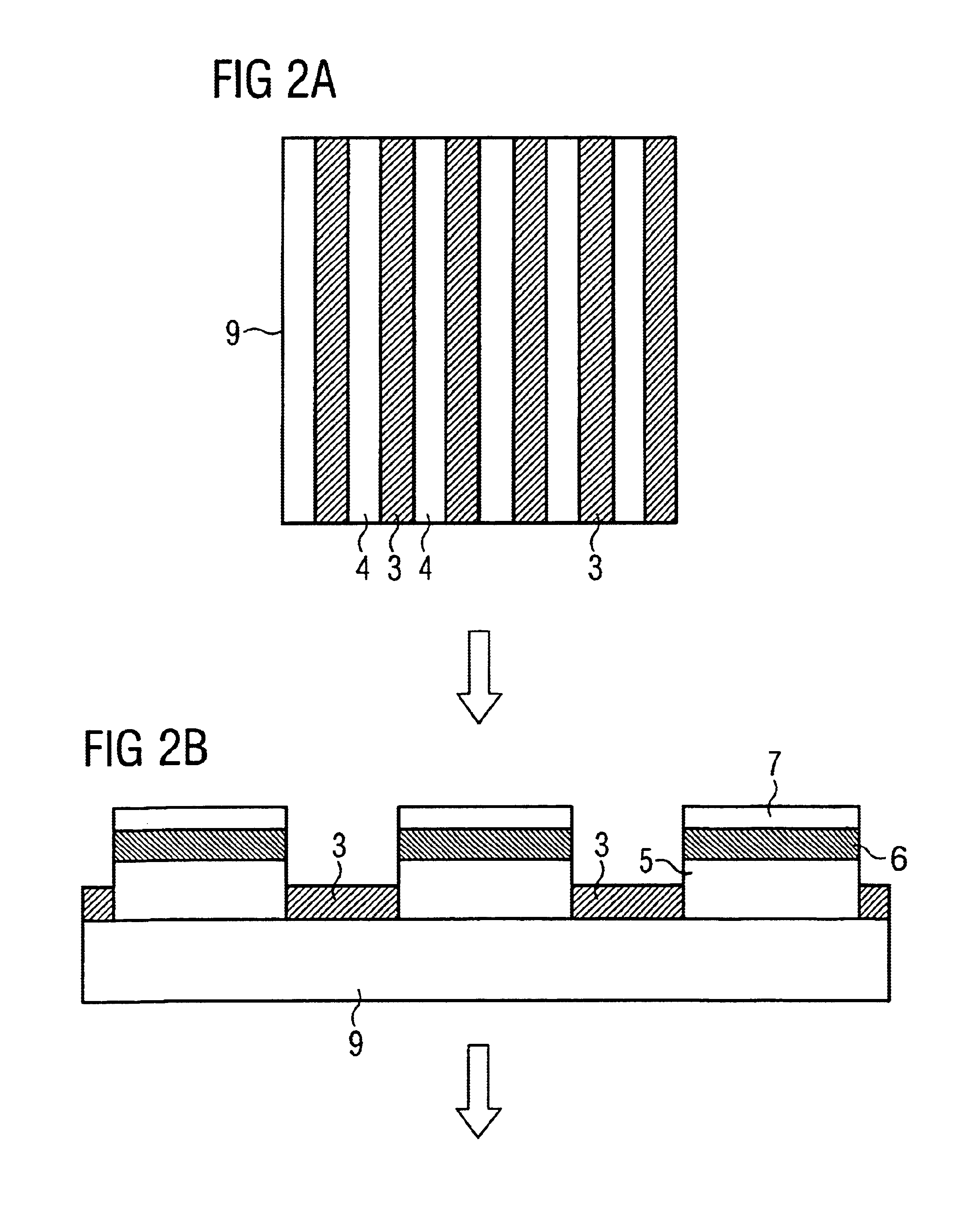
Reference is now made to the figures of the drawings in which elements that are identical or function identically are identified by the same reference numerals throughout. Prior to the start of any of the methods to be described below, it is within the scope of each to clean the epitaxial substrate, prior to any applications, with the introduction of at least one fluoride based hydrogen fluoride soluble layer. The cleaning may occur within or outside the epitaxy reactor. In FIGS. 1a-1c, an epitaxy substrate a is depicted with a masking layer 3 comprising one of a HF soluble material. Such material may be SiO2 or Si8N8. The masking layer 3 defines windows 4. The substrate, it not already present, is placed in an epitaxy reactor. Herein and as depicted in FIG. 1b, a layering sequence 10 is commenced in title windows 4. The sequence may be a semiconductor laser effected by MOVPE (metal organic vapor phase epitaxy). The application step is further indicated by arrows 11. Next and as dep...


PUM


Abstract

The present invention relates to a method for the production of semiconductor components. This method comprises the steps of applying masking layers and components on epitaxial semiconductor substrates within the epitaxy reactor without removal of the substrate from the reactor. The masking layers may be HF soluble such that a gas etchant may be introduced within the reactor so as to etch a select number and portion of masking layers. This method may be used for production of lateral integrated components on a substrate wherein the components may be of the same or different type. Such types include electronic and optoelectronic components. Numerous masking layers may be applied, each defining particular windows intended to receive each of the various components. In the reactor, the masks may be selectively removed, then the components grown in the newly exposed windows.

Description

BACKGROUND OF THE INVENTION1. Field of the InventionThe present invention relates to a method for manufacturing semiconductor components wherein HF (hydrogen fluoride) soluble masking material is used. The components may be optoelectronic or electronic semiconductor components or laterally integrated semiconductor components wherein electrical and optoelectronic semiconductor components are individually used or combined.2. Description of Related ArtIt is known in the art that HF soluble layers on an epitaxial substrate, such as a semiconductor substrate, may be chemically (wet or dry) removed outside of an epitaxial reactor. By this method, laterally integrated components may be produced by selective epitaxy or heteroepitaxy.In selective epitaxy, HF soluble layers are used for masking. Select layers are grown in the epitaxy reactor and thereafter, masked areas are chemically (wet or dry) removed outside of the reactor. For further integration's, additional lithographic steps would b...

Claims


Application Information

Patent Timeline
Patent Type & Authority Patents(United States)
IPC IPC(8): H01L21/02H01L21/306H01L21/20H01L21/205H01S5/02H01S5/026
CPCH01L21/30604
Inventor HARLE, VOLKER
Owner OSRAM OPTO SEMICON GMBH & CO OHG
Learn More