System for oxide stress testing

a stress testing and oxide technology, applied in the field of semiconductor devices, can solve the problems of reducing the performance or lifetime of the device, affecting the reliability of the device, and generating numerous challenges to the semiconductor manufacturing process, and achieves the effects of convenient, efficient and reliable assessment, and reduced manufacturing costs

Active Publication Date: 2005-03-08
TEXAS INSTR INC
View PDF5 Cites 15 Cited by
  • Summary
  • Abstract
  • Description
  • Claims
  • Application Information

AI Technical Summary

Benefits of technology

The present invention provides a versatile system of methods and structures that accurately characterize overstress behavior of oxide structures without altering device functionality—providing efficient and reliable assessment of semiconductor oxide integrity in an easy, efficient and cost-effective manner while overcoming limitations associated with previous approaches.
Specifically, the present invention provides circuitry that supplies a gate oxide overstress voltage (hereinafter referred to as overstress supply circuitry) that is independent of the operational gate supply. This circuitry may supply overstress voltage to a number of disparate FET structures—providing considerable space savings in device layout. The present invention further provides FET power-off discharge circuitry that may be implemented with the overstress supply circuitry or independent of such circuitry. The present invention provides this and other circuitry to remove alternative leakage paths during overstress testing while remaining operationally transparent during normal device operation—providing a more accurate and reliable overstress evaluation of a device.

Problems solved by technology

The increased packing density of the integrated circuit generates numerous challenges to the semiconductor manufacturing process.
Frequently, however, end equipment applications may, intentionally or not, require a semiconductor device to operate at some value outside the specified boundary parameters for a period (or periods) of time.
This operational overstress may degrade the performance or lifetime of the device, or may cause complete device failure.
In either case, system reliability is impacted significantly.
One such overstress problem, frequently encountered, involves over-voltage effects on semiconductor dielectrics—particularly oxides.
Depending upon the structures and processes with which a device is formed, certain dielectric structures and substructures can be especially susceptible to over-voltage damage.
Over-voltage operation can cause anomalies in a gate oxide (e.g., cracks, breaks)—anomalies that can alter or ruin the functionality of the FET.
Unfortunately, depending upon the specific circuitry implemented in the semiconductor device, there are often a number of device structures and substructures that interfere with or prevent the screening tests referenced above.
Some devices may incorporate circuitry (e.g., Zener diode) that couples the gate and the source of a FET together—limiting the extent to which the gate oxide may be stressed.
Certain devices lack blocking circuitry between the so gate and an operational supply that drives the gate during normal operation.
Thus, during gate oxide testing, a current path exists that may charge the supply—again limiting the extent to which the gate oxide may be stressed.

Method used


Image

  • System for oxide stress testing
  • System for oxide stress testing
  • System for oxide stress testing

Examples


Embodiment Construction

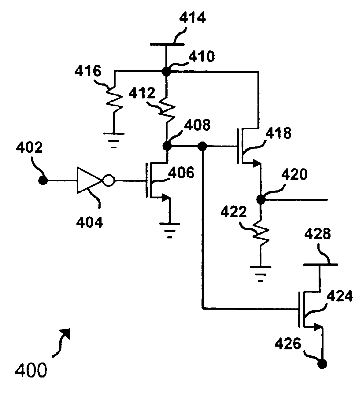
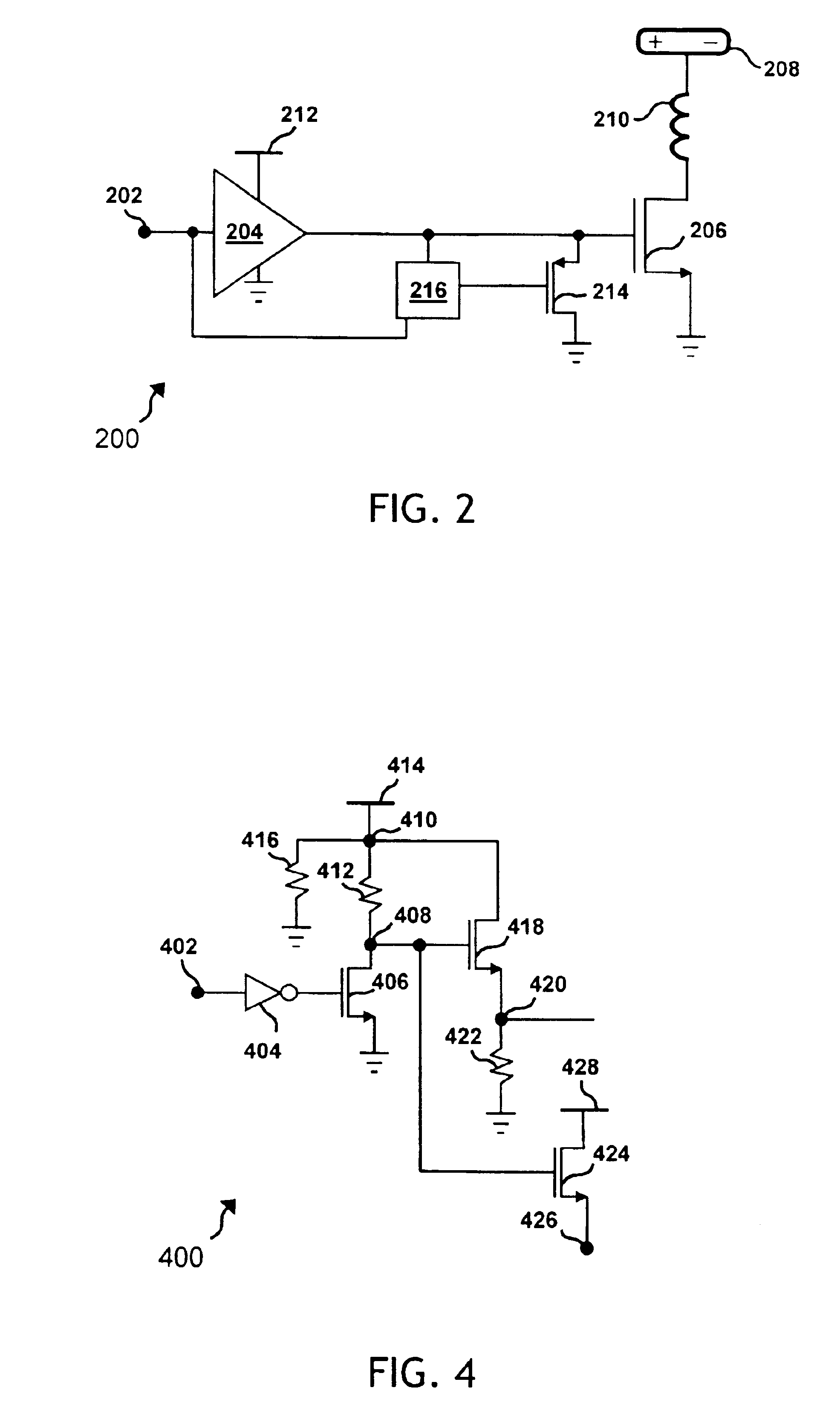
While the making and using of various embodiments of the present invention are discussed in detail below, it should-be appreciated that the present invention provides many applicable inventive concepts, which can be embodied in a wide variety of specific contexts. The invention will now be described in conjunction with the over-voltage testing of a gate oxide structure. The specific embodiments discussed herein are, however, merely illustrative of specific ways to make and use the invention and do not limit the scope of the invention.

The system of the present invention provides accurate characterization of oxide overstress behavior, without altering device functionality. Utilizing this system, efficient and reliable assessment of semiconductor oxide integrity is provided in an easy, efficient and cost-effective manner. Specifically, the present invention provides circuitry that supplies a gate oxide overstress voltage (hereinafter referred to as overstress supply circuitry) that is ...


PUM


Abstract

The present invention provides a system for stress testing an oxide structure to determine that structure's reliability in overstress conditions. The present invention provides an overstress test structure (400) that comprises a first transistor (406), having a first terminal coupled to ground, a second terminal coupled to a control signal (402), and a third terminal coupled to a first end of a first resistive element (412). A first voltage source (414) is coupled to the second end of the first resistive element. A second resistive element (416) is intercoupled between the second end of the first resistive element and ground. A second transistor (418) has a first terminal coupled to the second end of the first resistive element, a second terminal coupled to the first end of the first resistive element, and a third terminal coupled to a first node (420). A third resistive element (422) is intercoupled between the third terminal of the second transistor and ground; and a third transistor (424) has a first terminal coupled (426) to the oxide structure, a second terminal coupled to the first end of the first resistive elerment, and a third terminal coupled to a second voltage source (428).

Description

TECHNICAL FIELD OF THE INVENTIONThe present invention relates generally to the field of semiconductor devices and, more particularly, to apparatus and methods for stress testing gate oxide integrity in semiconductor devices.BACKGROUND OF THE INVENTIONThe continual demand for enhanced integrated circuit performance has resulted in, among other things, a dramatic reduction of semiconductor device geometries, and continual efforts to optimize the performance of every substructure within any semiconductor device. A number of improvements and innovations in fabrication processes, material composition, and layout of the active circuit levels of a semiconductor device have resulted in very high-density circuit designs. Increasingly dense circuit design has not only improved a number of performance characteristics, it has also increased the importance of, and attention to, semiconductor material properties and behaviors.The increased packing density of the integrated circuit generates numer...

Claims


Application Information

Patent Timeline
Patent Type & Authority Patents(United States)
IPC IPC(8): G01R31/28
CPCG01R31/2858
Inventor TEGGATZ, ROSS E.ADAMS, REED W.RAJASEKHAR, SURIBHOTLA V.
Owner TEXAS INSTR INC
Why Eureka
Try Eureka