Method of forming patterned nickel and doped nickel films via microcontact printing and uses thereof

Inactive Publication Date: 2005-03-15
IBM CORP
View PDF2 Cites 20 Cited by
  • Summary
  • Abstract
  • Description
  • Claims
  • Application Information

AI Technical Summary

Benefits of technology

Another general purpose of the invention is to provide electronic and optical elements and devices t

Problems solved by technology

While the above-described irradiative lithographic methods may be advantageous in many circumstances, all require relatively sophisticated and expensive apparatus to reproduce a particular pattern on a plurality of substrates.
Additionally, they generally consume more reactants and produce more by

Method used


Image

  • Method of forming patterned nickel and doped nickel films via microcontact printing and uses thereof
  • Method of forming patterned nickel and doped nickel films via microcontact printing and uses thereof
  • Method of forming patterned nickel and doped nickel films via microcontact printing and uses thereof

Examples


example 1

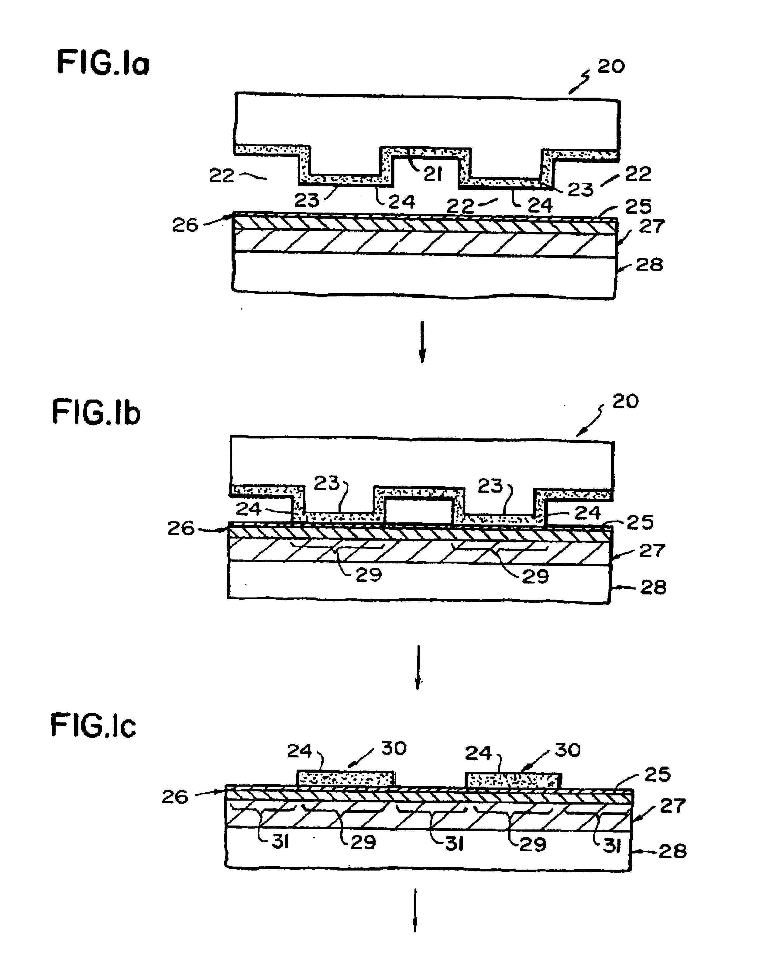
Fabrication of a Microcontact Printing Stamp

A template consisting of an exposed and developed photoresist pattern was fabricated by photolithography. A 2-mm-high border was formed by fixing strips of 2-mm-thick adhesive-backed foam around the perimeter of the surface of the template. A 10:1 (w:w or v:v) mixture of PDMS-Sylgard Silicone Elastomer 184 and Sylgard Curing Agent 184 (Dow Corning Corp., Midland, Mich.) was degassed under vacuum for about 10 minutes, then the mixture was poured over the template to approximately the height of the foam border. The PDMS cured at 65° C. for 60 minutes. After cooling to room temperature, the PDMS-stamp was carefully peeled from the template.

example 2

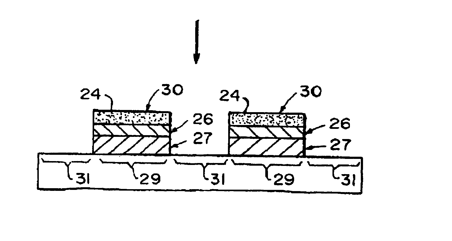
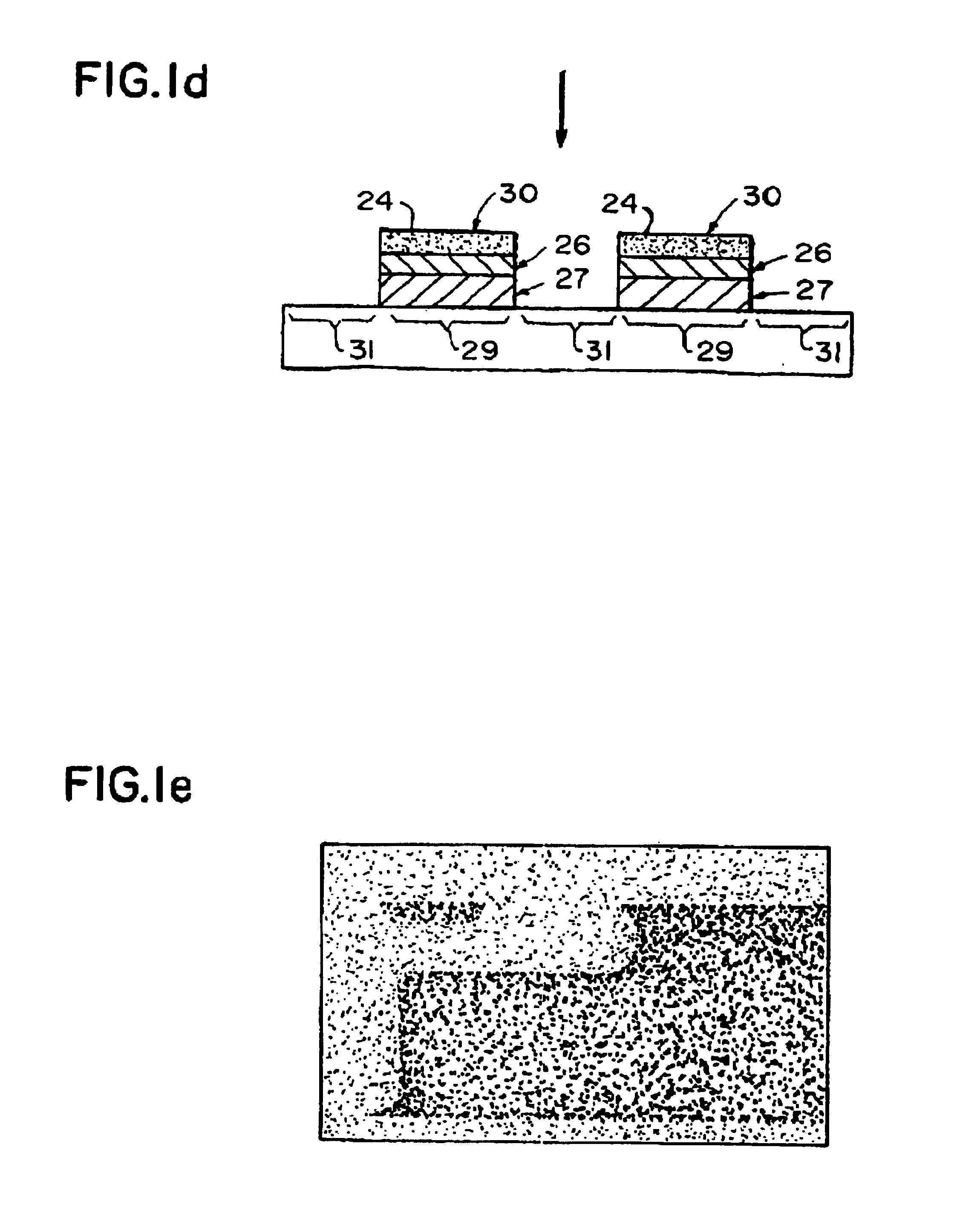
Patterning Boron-Doped Nickel Films by Microcontact Printing and Wet Etching

A stamp fabricated in accordance with Example 1 was fabricated. The surface was coated with octadecylphosphonic acid in ethanol by applying a small volume of solution to cover the surface of the stamp. After allowing the solution to contact the surface of the stamp for 30s, the stamp surface was dried under a stream of dry dinitrogen. The stamp was applied to the native nickel oxide surface of a boron-doped nickel film and removed, whereby a pattern of alkanephosphonic acid is formed. The remaining unprotected native nickel oxide layer and boron-doped nickel film was removed from the surface of the silicon substrate using an aqueous hydrochloric acid (8.0 mM) and hydrogen peroxide (0.6% v:v) solution, thus transferring the pattern of the stamp to the native nickel oxide layer and boron-doped nickel film. An optical micrograph of the resultant pattern is shown in FIG. 2a and a scanning electron micrograph in ...


PUM

PropertyMeasurementUnit
Thicknessaaaaaaaaaa
Thicknessaaaaaaaaaa
Molar densityaaaaaaaaaa

Abstract

The process of derivatization and patterning of surfaces, and more particularly to the formation of self-assembled molecular monolayers on metal oxide surfaces using microcontact printing and the derivative articles produced thereby.

Description

FIELD OF THE INVENTIONThe present invention relates generally to derivatization and patterning of surfaces, and more particularly to the formation of self-assembled molecular monolayers on metal oxide surfaces using microcontact printing and derivative articles produced thereby.BACKGROUNDIn the field of microelectronic devices, sensors, optical elements and electronic displays, the development of devices that are conveniently and relatively inexpensively produced with a relatively low failure rate is important.A well-known method of production of such devices is photolithography. According to this technique, a negative or positive resist (photoresist) is coated onto the exposed surface of a substrate. The resist is then irradiated in a predetermined pattern, and irradiated (positive resist) or non irradiated (negative resist) portions of the resist are washed from the surface to produce a predetermined pattern of resist on the surface. This is followed by one or more procedures. For...

Claims


Application Information

Patent Timeline
IPC IPC(8): C23F1/02C23F1/28C23F1/10B05D1/28B81C1/00G03F7/00
CPCB81C1/0046B82Y10/00G03F7/0002B82Y40/00C23F1/02C23F1/28B82Y30/00B05D1/283
Inventor BREEN, TRICIA L.FRYER, PETER M.WISNIEFF, ROBERT L.FLAKE, JOHN CHRISTOPHER
Owner IBM CORP
Why Eureka
Try Eureka