Semiconductor device

a technology of semiconductor devices and internal leads, applied in semiconductor devices, semiconductor/solid-state device details, electrical apparatus, etc., can solve the problems of difficulty in further improving fine pitch, difficulty in realizing fine pitch improvement, and lowering so as to improve the fine pitch of inner leads and improve the bonding accuracy of inner leads

Active Publication Date: 2005-03-15
SHENZHEN TOREY MICROELECTRONIC TECH CO LTD
View PDF7 Cites 51 Cited by
  • Summary
  • Abstract
  • Description
  • Claims
  • Application Information

AI Technical Summary

Benefits of technology

An object of the present invention is to provide a semiconductor device which can realize improvement in f

Problems solved by technology

However, reduction in distance between the bump electrodes 19 or reduction in width of the bump electrode 19 causes a problem of lowering a bonding accuracy in bonding between the bump electrode 19 and an inner lead 11.
That is, in thermocopression bonding, due to the shifted position of the inner lead 11, the inner lead 11 comes into contact with a bump electrode which is not an intended bump electrode 19 to be bonded with, resulting in shorts and lead defects.
10(a), reduction in distance between the bump electrodes 19 or reduction in width of the bump electrode 19 might cause shorts and leak defects, which results in the difficulty of further improvement in fine pitch.
However, ther

Method used


Image

  • Semiconductor device
  • Semiconductor device
  • Semiconductor device

Examples


embodiment 1

The following will describe one embodiment of the present invention with reference to FIG. 1 through FIG. 4.

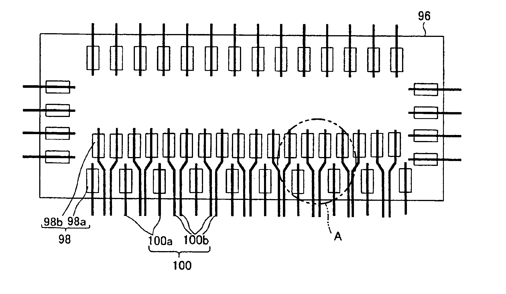
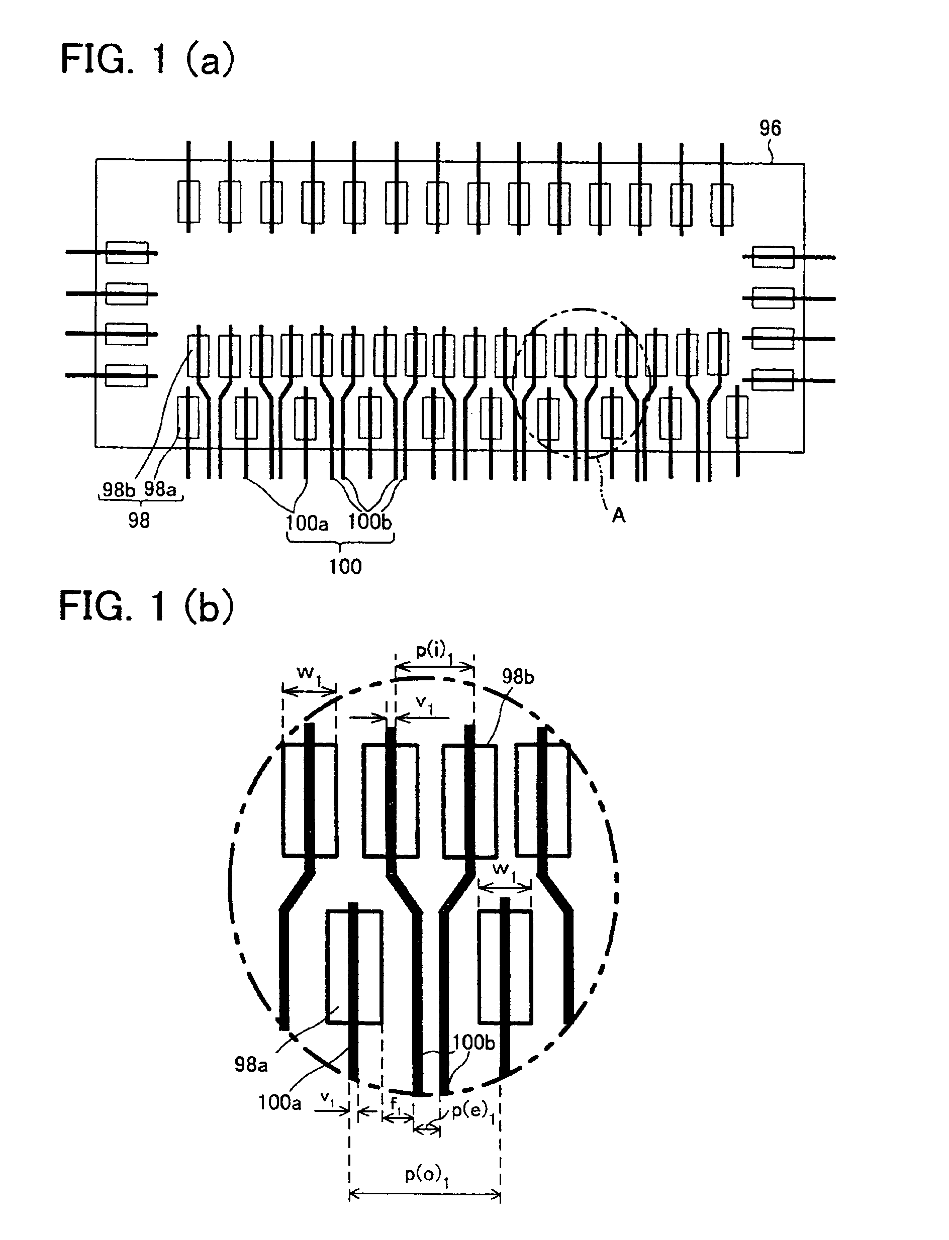
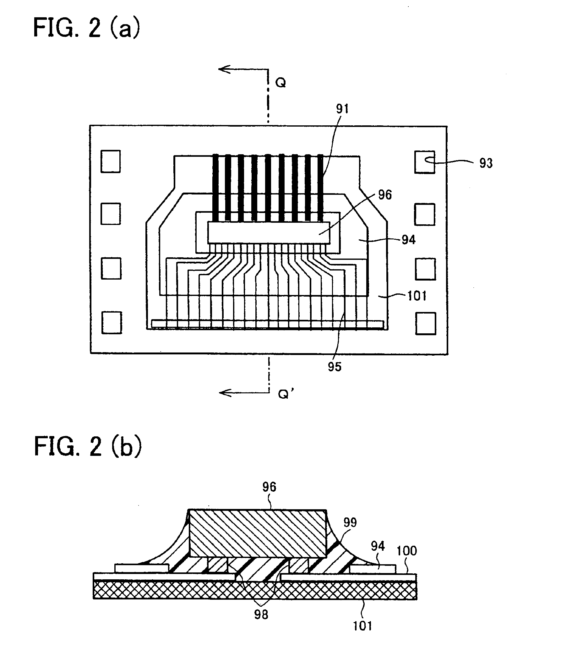
As shown in FIG. 2(b), a COF (Chip On Film; semiconductor device) of the present embodiment includes an inner lead (lead wire) 100 supported by a film substrate 101 and a bump electrode 98 provided to a semiconductor chip 96 which are placed so as to be opposed each other and to be electrically connected to each other.

On the inner lead 100 provided on the film substrate 101, formed is a solder resist 94 as protective film made of polyimide or polyurethane material having high heat resistance. The solder resist 94 is provided to prevent damage to the inner lead 100 such as corrosion and leak failure, caused by the adhesion of conductive or ionic foreign substance. The solder resist 94 also prevents the inner lead 100 from be broken by external force and protects the inner lead 100 in the process of bending. Note that, the solder resist 94 is formed to a thickness of 3 μm to 30 ...

embodiment 2

The following will describe another embodiment of the present invention with reference to FIG. 5. Note that, for the purpose of explanation, members having the same functions as those illustrated in drawings of Embodiment 1 are given the same reference numerals and explanations thereof are omitted here.

In a semiconductor chip 96 of the present embodiment, as shown in FIG. 5(a), bump electrodes spaced at predetermined pitches are arranged in three rows respectively at different distances from the end of the semiconductor chip 96. Hereinafter, the bump electrodes arranged in three rows are referred to as a first bump electrode (edge-side bump electrode) 68a, a second bump electrode (first inner-side bump electrode) 68b, and a third bump electrode (second inner-side bump electrode) 68c in the order of being relatively small distance apart from the end of the semiconductor chip 96. When any one or all of the first bump electrode 68a, the second bump electrode 68b, and the third bump ele...

embodiment 3

The following will describe still another embodiment of the present invention with reference to FIG. 6 and FIG. 7. Note that, for the purpose of explanation, members having the same functions as those illustrated in drawings of Embodiments 1 and 2 are given the same reference numerals and explanations thereof are omitted here.

In a COF of the present embodiment, some of the inner-side bump electrodes 58b in the COF shown in FIG. 4(a), which has been described in Embodiment 1, are placed so as to be different from the others in distance from the end of the semiconductor chip 96. More specifically, as shown in FIG. 6, a bump electrode 77 is placed at a position more distant than the position of the inner-side bump electrode 58b from the end of the semiconductor chip 96. Moreover, the bump electrode 77 is placed in a different direction from a direction in which the outer-side bump electrode 58a and the inner-side bump electrode 58b are provided. That is, the bump electrode 77 is so pro...


PUM


Abstract

A semiconductor device of the present invention has two inner inner leads to be bonded with inner-side bump electrodes each placed at a position which is a relatively large distance apart from the edge of a semiconductor chip, between outer-side bump electrodes each placed at a position which is a relatively small distance apart from the edge of the semiconductor chip. At least one of the inner inner leads is bent in accordance with a bonding position with the inner-side bump electrode.

Description

This Nonprovisional application claims priority under 35 U.S.C. § 119(a) on Patent Application No. 2002 / 357089 filed in Japan on Dec. 9, 2002, the entire contents of which are hereby incorporated by reference.FIELD OF THE INVENTIONThe present invention relates to a semiconductor device, and more specifically, to a semiconductor device having inner leads provided at a fine pitch.BACKGROUND OF THE INVENTIONA COF (Chip On Film) in which a semiconductor chip made up of LSI and other components is mounted on a film substrate is used as a package for liquid crystal driver. In case of the COF, bump electrodes are provided at a predetermined alignment pitch in a periphery of the semiconductor chip. These bump electrodes are bonded with the inner leads to connect between the semiconductor chip and the film substrate. That is, as shown in FIG. 9(a), bump electrodes 18 are provided on a semiconductor chip 16, and the bump electrodes 18 are connected respectively to inner leads 10 supported by ...

Claims


Application Information

Patent Timeline
IPC IPC(8): H01L21/56H01L21/02H01L23/498H01L23/48H01L21/60
CPCH01L21/563H01L23/49838H01L23/4985H01L2224/73203H01L2924/01078H01L2924/01079H01L2924/15173H01L2224/73204H01L2224/32225H01L2224/16225H01L2924/00H01L2924/00014H01L2224/0401H01L23/48
Inventor TOYOSAWA, KENJI
Owner SHENZHEN TOREY MICROELECTRONIC TECH CO LTD
Why Eureka
Try Eureka