Half-rate clock logic block and method for forming same

a logic block and half-rate clock technology, applied in the field of combinatorial and sequential logic circuits, can solve the problems of insufficient time for a circuit element, output signal may be erroneous, and difficulty in converting to a half-rate clock

Inactive Publication Date: 2005-03-15
AVAGO TECH INT SALES PTE LTD
View PDF4 Cites 16 Cited by
  • Summary
  • Abstract
  • Description
  • Claims
  • Application Information

AI Technical Summary

Problems solved by technology

As the period of each clock cycle decreases, there may be insufficient time for a circuit element (such as a gate) to perform its function during the interval between the active edge of two successive clock cycles.
That is, when the clock period is less than the combined set up and hold time of a synchronous circuit element the output signal maybe erroneous.
The conversion process from the full rate to the half-rate design can be a time consuming task Control circuits or other circuits having a considerable number of full-rate feedback paths can be difficult to convert to a half-rate system.
For example, converting a full-rate state machine to half-rate operation is a complex and time-consuming process, since there are a plurality of states and each state has several feed-forward paths.
Thus the results of the conversion process often vary considerably in terms of the circuit area consumed on an integrated circuit device in which the design is implemented, power consumption, and overall effectiveness of the half-rate design when compared with its full-rate counterpart.

Method used


Image

  • Half-rate clock logic block and method for forming same
  • Half-rate clock logic block and method for forming same
  • Half-rate clock logic block and method for forming same

Examples


Embodiment Construction

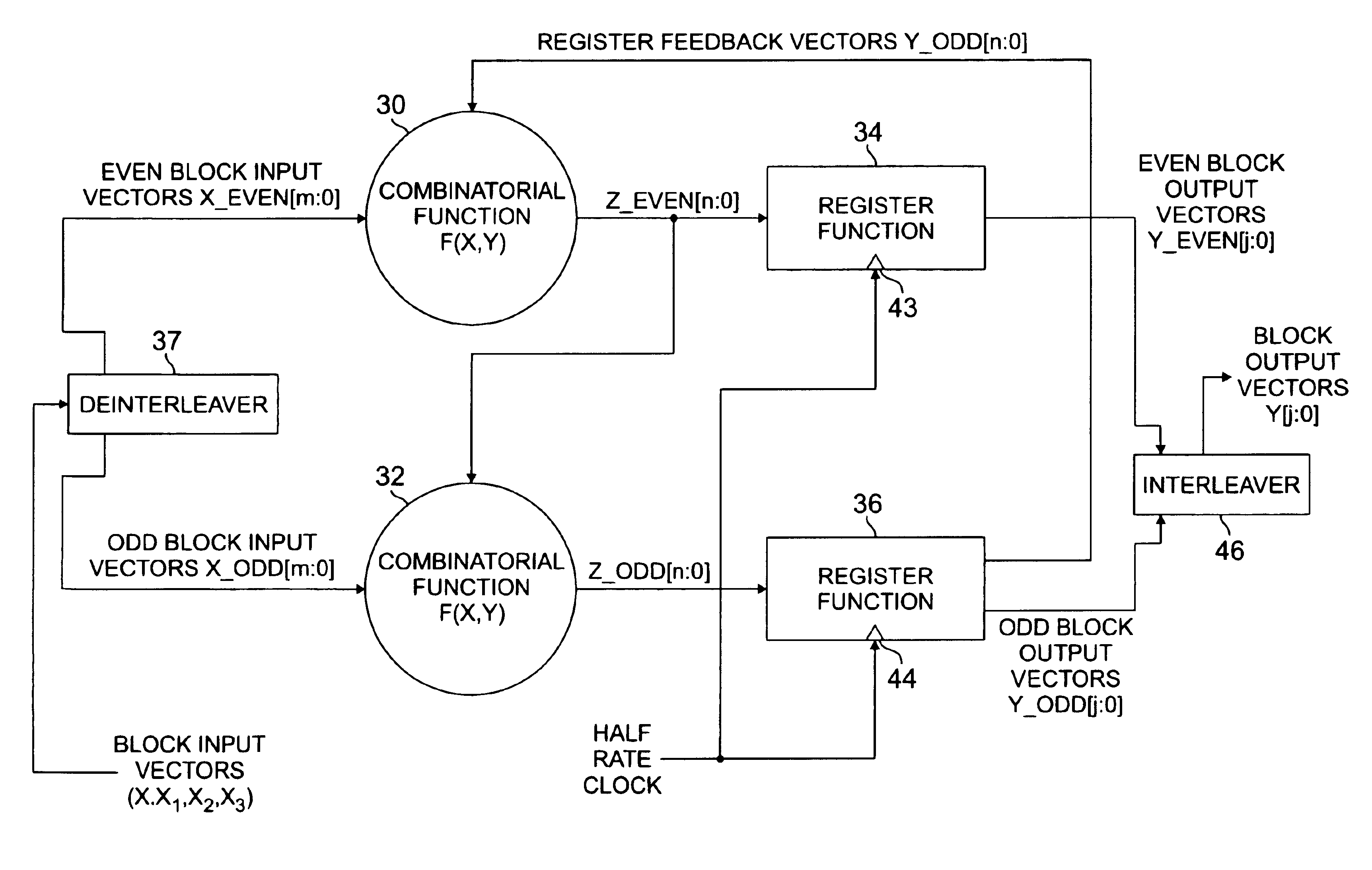
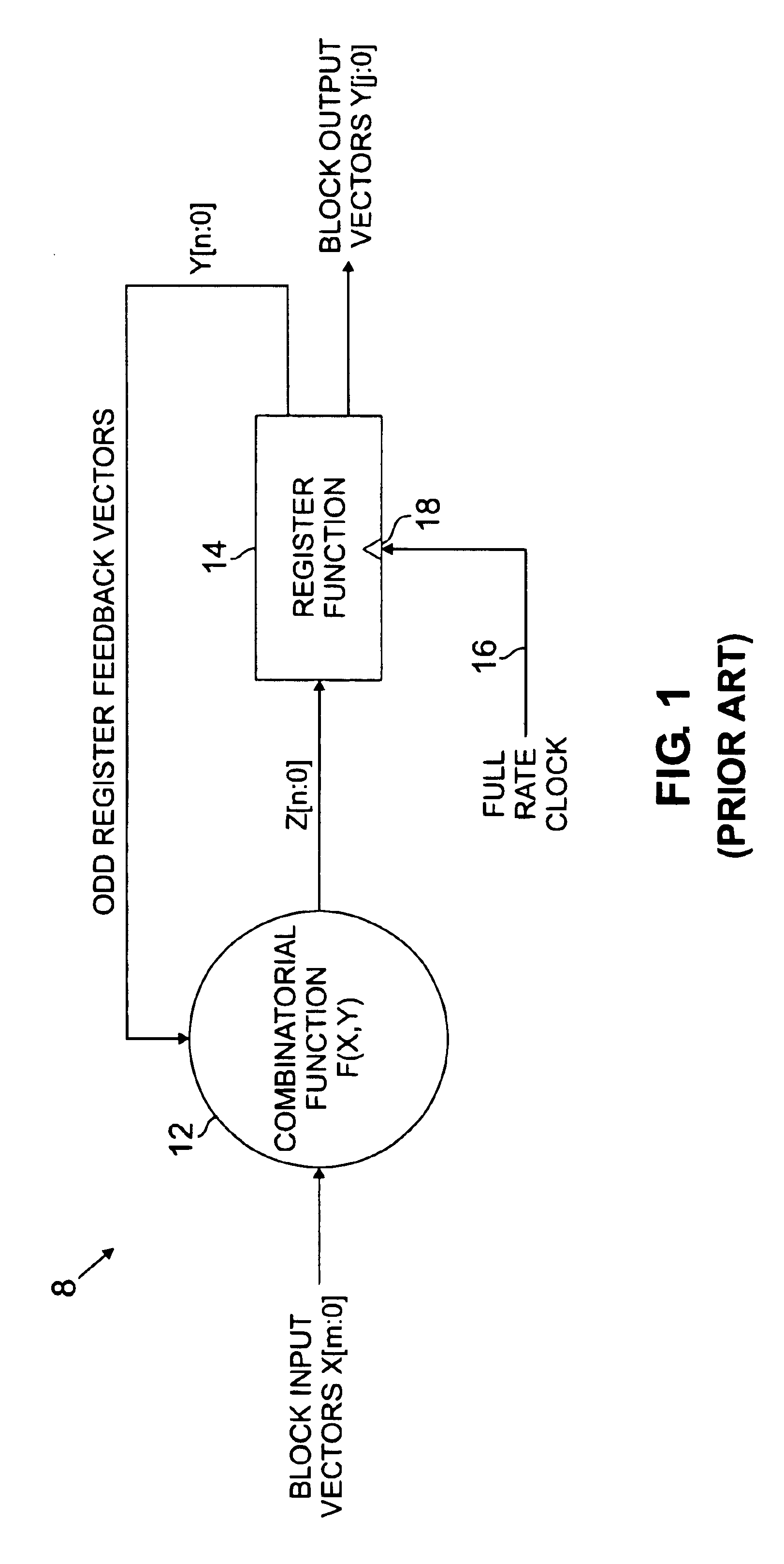
Before describing in detail the particular half-rate clock digital circuitry and the method for converting a full-rate clock digital circuit to a half-rate clock circuit in accordance with the present invention, it should be observed that the present invention resides primarily in a novel and non-obvious combination of elements and method steps. Accordingly, these elements and steps have been represented by conventional elements in the drawings, showing only those specific details that are pertinent to the present invention so as not to obscure the description with structural details that will be readily apparent to those skilled in the art having the benefit of the description herein.

FIG. 1 illustrates a prior art full-rate clock logic block 8 comprising a combinatorial function 12 and a register function 14 (also referred to as a sequential function). A plurality of m+1 logic signals (designated 0, 1, 2 . . . m) comprise a signal vector X (designated X[m:0], input to the combinato...


PUM


Abstract

A method and apparatus for converting a full-rate digital clock circuit to a fractional-rate clock circuit. The combinatorial and sequential functions of the full rate design are duplicated, with a first combinatorial function responsive to even input logic vectors and a second combinatorial function responsive to odd input logic vectors. Output vectors from the first and the second combinatorial function are provided as input vectors to the respective first and second sequential function, which operate at a fractional clock rate and provide the output block vectors.

Description

FIELD OF THE INVENTIONThe present invention relates to combinatorial and sequential logic circuits, and more particularly to combinatorial and sequential logic circuits operating at a fractional clock rate.BACKGROUND OF THE INVENTIONCombinatorial logic devices produce one or more output signals in response to logical combinations of one or more input signals. Thus, combinatorial networks can function to indicate the presence of a given set of input signals by producing a corresponding output signal. Decoders, adders, logic gates and shifters are examples of combinatorial logic networks. A simple exemplary decoder produces an output signal indicating the state of two input variables. Since there are four possible combinations of two binary input variables, the input state can be determined by a decoder capable of producing one of four output signals. The output signal thus indicates or decodes the input state. Combinatorial networks are conventionally built from basic logic circuits ...

Claims


Application Information

Patent Timeline
Patent Type & Authority Patents(United States)
IPC IPC(8): H03K19/173H03K19/00G06F9/38
CPCG06F9/3875G06F9/3869
Inventor GRUNDVIG, JEFFREY PAUL
Owner AVAGO TECH INT SALES PTE LTD
Why Eureka
Try Eureka