Semiconductor memory device, and method of controlling the same
- Summary
- Abstract
- Description
- Claims
- Application Information
AI Technical Summary
Benefits of technology
Problems solved by technology
Method used
Image
Examples
first embodiment
FIG. 3 shows the semiconductor memory device and its control method in the present invention. The semiconductor memory device of this embodiment is formed as a DRAM on a p-type silicon substrate by employing the CMOS process technology.
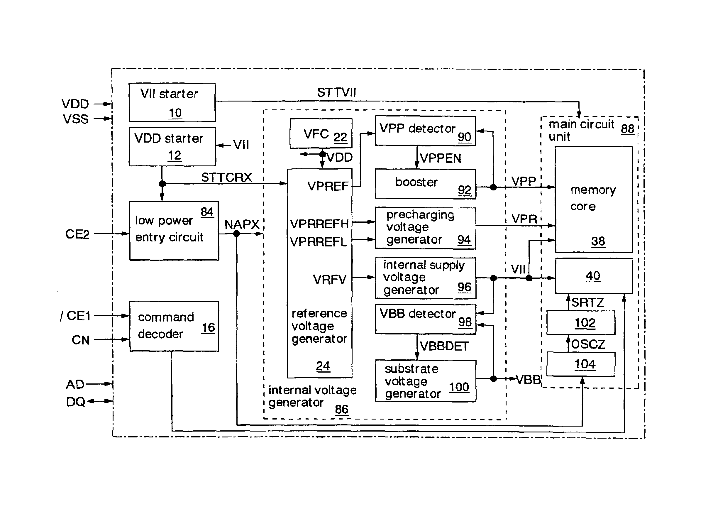
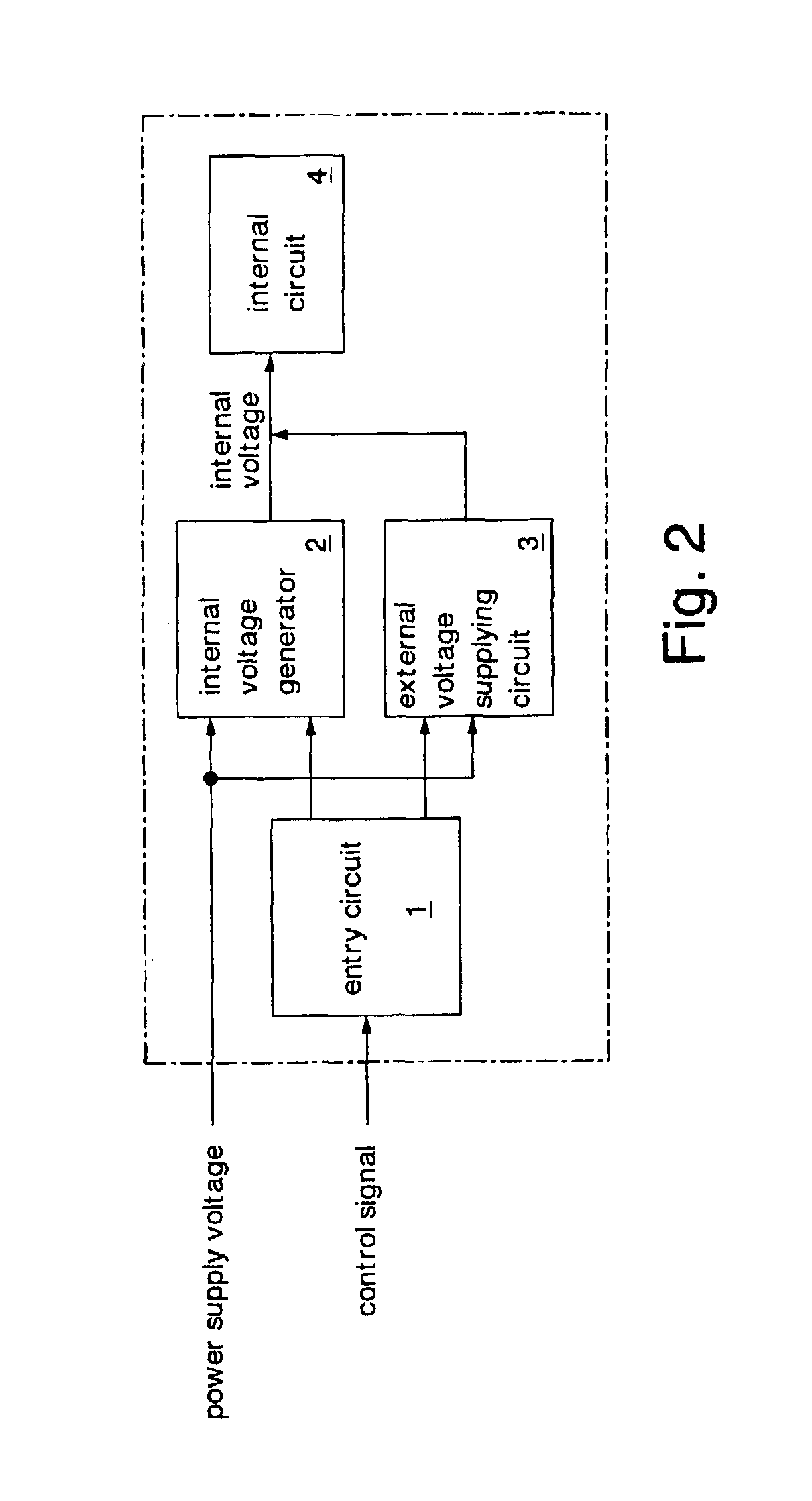
The DRAM is provided with a VII starter 10, a VDD starter 12, a low power entry circuit 14, a command decoder 16, an internal voltage generator 18 and a main circuit unit 20. The internal voltage generator 18 has a low-pass filter 22, a reference voltage generator 24, a VDD supplying circuit 26, a booster 28, a precharging voltage generator 30, an internal supply voltage generator 32, a substrate voltage generator 34 and a VSS supplying circuit 36. The main circuit unit 20 has a memory core 38 and a peripheral circuit 40. Here, the low power entry circuit 14 corresponds to the entry circuit 1 shown in FIG. 2, and the VDD supplying circuit 26 and the VSS supplying circuit 36 correspond to the external voltage supplying circuit 3 shown in FIG. 2.
The DRA...
fourth embodiment
This embodiment can also achieve effects similar to those of the foregoing In this embodiment, moreover, at the time of the exit from the low power consumption mode a start signal STTVII for initializing an internal circuit is activated during a period where the boost voltage VPP internally generated is lower than the power supply voltage VDD from the exterior. Specifically, at the time of the exit from the low power consumption mode, the start signal STTVII for initializing an internal circuit is activated during a period where at least one of the internal power supply voltage VII and is / are respectively lower than the reference voltage VREF and the power supply voltage VDD. This makes it possible to securely reset the internal circuit and prevent the malfunction of the internal circuit when the low power consumption mode shifts to the normal operating mode.
FIG. 20 shows a start signal generator of the semiconductor memory device in a sixth embodiment and its control method of a f...
third embodiment
The foregoing third embodiment has been described on the example using the dedicated low power consumption mode signal / LP. This DRAM can be supplied even to the user requiring no low power consumption mode, for example, by pulling up the / LP signal on the chip and providing no terminal for the / LP signal. This / LP signal may be connected with the power supply voltage VDD by bonding or blowing the fuse. Alternatively, the / LP signal may be connected with the power supply voltage VDD by selecting photo masks of a wiring layer.
PUM
 Abstract
Description
Claims
Application Information


