Method for fabricating a photonic crystal

a technology of photonic crystals and manufacturing methods, applied in the manufacture of electrode systems, cold cathode manufacturing, electric discharge tubes/lamps, etc., can solve the problems of inherently less efficiency in converting input electrical power, the least efficient (energy to useful light) lighting technology used commercially today, and the least efficient (energy-to-use light) lighting technology used today

Inactive Publication Date: 2005-03-22
NAT TECH & ENG SOLUTIONS OF SANDIA LLC
View PDF12 Cites 27 Cited by
  • Summary
  • Abstract
  • Description
  • Claims
  • Application Information

AI Technical Summary

Benefits of technology

[0011]The present invention provides a photonically engineered incandescent emitter, comprising a photonic crystal having a characteristic lattice constant and comprising an emitter material having a first dielectric constant and at least one other lattice material having at least one other dielectric constant and wherein the characteristic lattice constant, the emitter material, and the at least one other lattice material are c

Problems solved by technology

They are also, unfortunately, the least efficient (energy to useful light) lighting technology used commercially today.
This disclosure will use the latter

Method used


Image

  • Method for fabricating a photonic crystal
  • Method for fabricating a photonic crystal
  • Method for fabricating a photonic crystal

Examples


Embodiment Construction

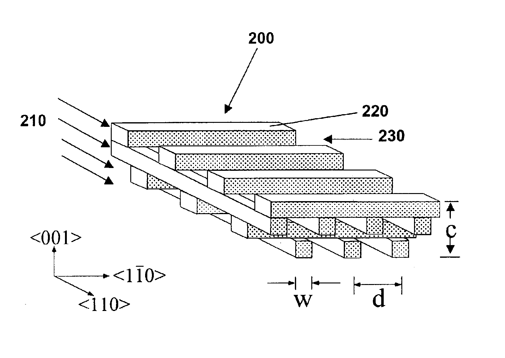
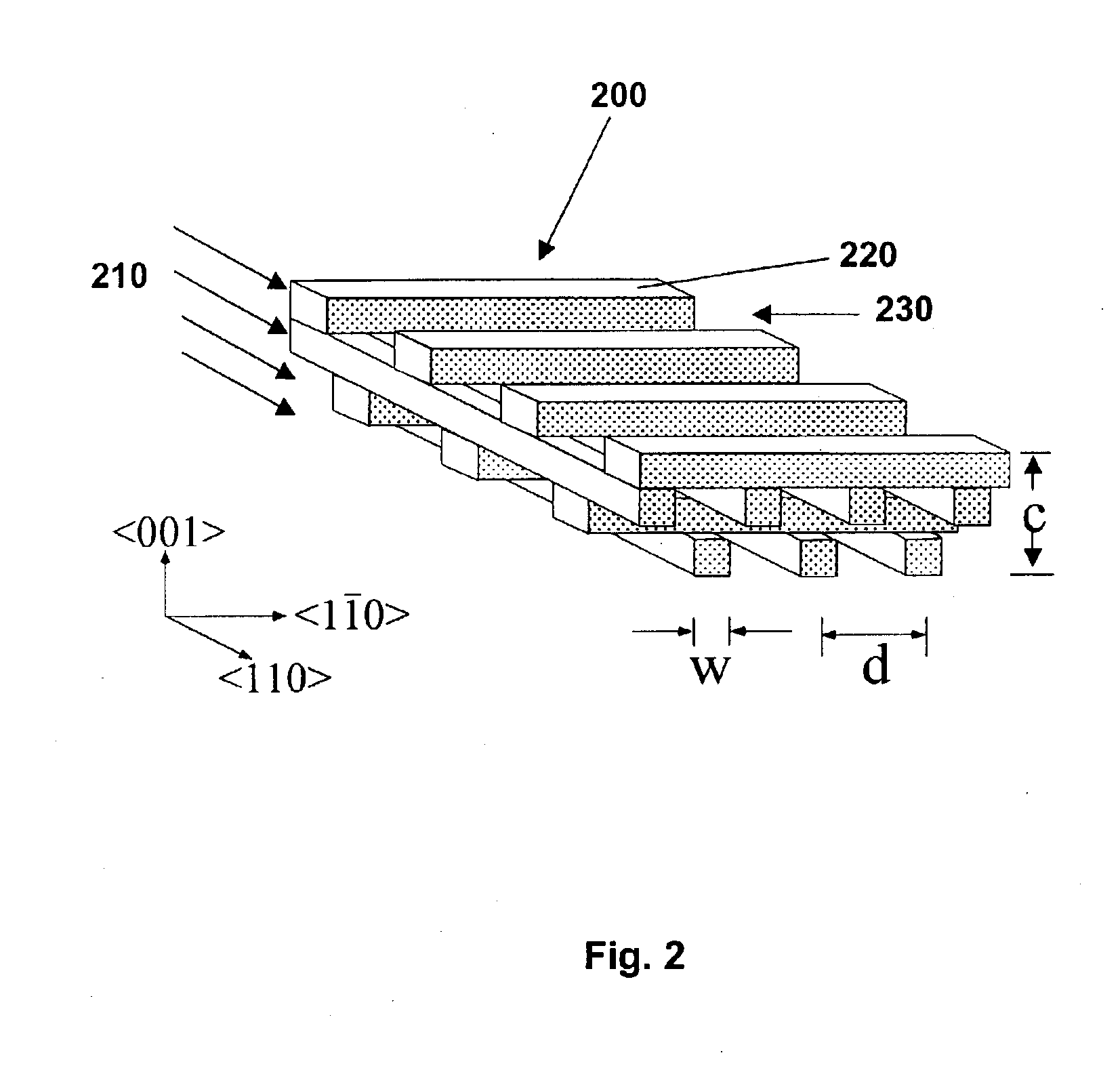
otonic crystal prior to removal of a silica sacrificial mold. FIG. 4b shows the tungsten photonic crystal after removal of the silica sacrificial mold. The one-dimensional tungsten rod used to form the crystal has a rod width of 1.2 μm and the rod-to-rod spacing of 4.2 μm.

[0018]FIG. 5 shows the measured reflectance and transmittance spectra for the light propagating along the axis of the four-layer tungsten photonic crystal.

[0019]FIG. 6 shows the tilt-angle reflectance spectra from the four-layer tungsten photonic crystal.

[0020]FIG. 7 shows the computed transmission spectra for tungsten photonic crystals with N=2, 4 and 6 layers.

[0021]FIG. 8 shows the spectral emissivity of the four-layer tungsten photonic crystal having a lattice constant of 4.2 μm.

DETAILED DESCRIPTION OF THE INVENTION

[0022]The present invention comprises a photonically engineered incandescent emitter that is more efficient than conventional incandescent lamps and a method for making the same. The more efficient i...


PUM


Abstract

A photonically engineered incandescence is disclosed. The emitter materials and photonic crystal structure can be chosen to modify or suppress thermal radiation above a cutoff wavelength, causing the emitter to selectively emit in the visible and near-infrared portions of the spectrum. An efficient incandescent lamp is enabled thereby. A method for fabricating a three-dimensional photonic crystal of a structural material, suitable for the incandescent emitter, is also disclosed.

Description

CROSS REFERENCE TO RELATED APPLICATIONS[0002]This is a divisional of application Ser. No. 09 / 940,962, filed Aug. 27, 2001 and since issued as U.S. Pat. No. 6,611,085.STATEMENT OF GOVERNMENT INTEREST[0003]This invention was made with Government support under contract no. DE-AC04-94AL85000 awarded by the U.S. Department of Energy to Sandia Corporation. The Government has certain rights in the invention.BACKGROUND OF THE INVENTION[0004]The present invention relates to incandescent lamps, and more particularly to incandescent lamps made from photonically engineered thermal emitters.[0005]Incandescent lamps offer very high quality lighting, are inexpensive, and are the most popular lighting technology for residential use. They are also, unfortunately, the least efficient (energy to useful light) lighting technology used commercially today. An excellent overview of incandescent lamp technology is given in Bergman et al., Filament Lamps, GE Research and Development Center, Report 98CRD027,...

Claims


Application Information

Patent Timeline
IPC IPC(8): H01L33/00H01K1/02H01K1/04H01K3/02H01L33/02
CPCH01K1/04H01K3/02H01L33/02H01K1/50
Inventor GEE, JAMES M.LIN, SHAWN-YUFLEMING, JAMES G.MORENO, JAMES B.
Owner NAT TECH & ENG SOLUTIONS OF SANDIA LLC
Why Eureka
Try Eureka