Semiconductor device and its manufacturing method

a manufacturing method and semiconductor technology, applied in semiconductor devices, electrical devices, transistors, etc., can solve the problems of low reliability of tunnel oxide films, difficult manufacturing methods, and difficult process, so as to improve memory cell characteristics, reduce electric field concentration in and increase the distance between the shoulder portion of the trench and the gate electrode.

Inactive Publication Date: 2005-03-22
RENESAS ELECTRONICS CORP
View PDF11 Cites 12 Cited by
  • Summary
  • Abstract
  • Description
  • Claims
  • Application Information

AI Technical Summary

Benefits of technology

According to the present embodiments, a semiconductor device includes memory cells isolated by a trench that may be self aligned with a stacked film pattern. The memory cells may be flash memory cells having an active gate film that may be thinner than a gate oxide film. The active gate film may be located in a central portion under of a gate electrode. The gate oxide film may be located under end portions of the gate electrode. In this way, a distance between a shoulder portion of a trench and a gate electrode may be increased. Thus, an electric field concentration in the shoulder portion of the trench may be decreased and memory cell characteristics may be improved.

Problems solved by technology

However, the conventional manufacturing method of a flash memory of this type can have problems.
First, the reliability of the tunnel oxide film can be low.
Second, the process can become complicated when forming the floating gate electrodes in a two-layered structure in order to implement a high capacitance ratio.
Thus, holding characteristics can be deteriorated resulting in a reduced reliability in the tunnel oxide film.
Doing so, may increase the area consumed by each memory cell.

Method used


Image

  • Semiconductor device and its manufacturing method
  • Semiconductor device and its manufacturing method
  • Semiconductor device and its manufacturing method

Examples


first embodiment

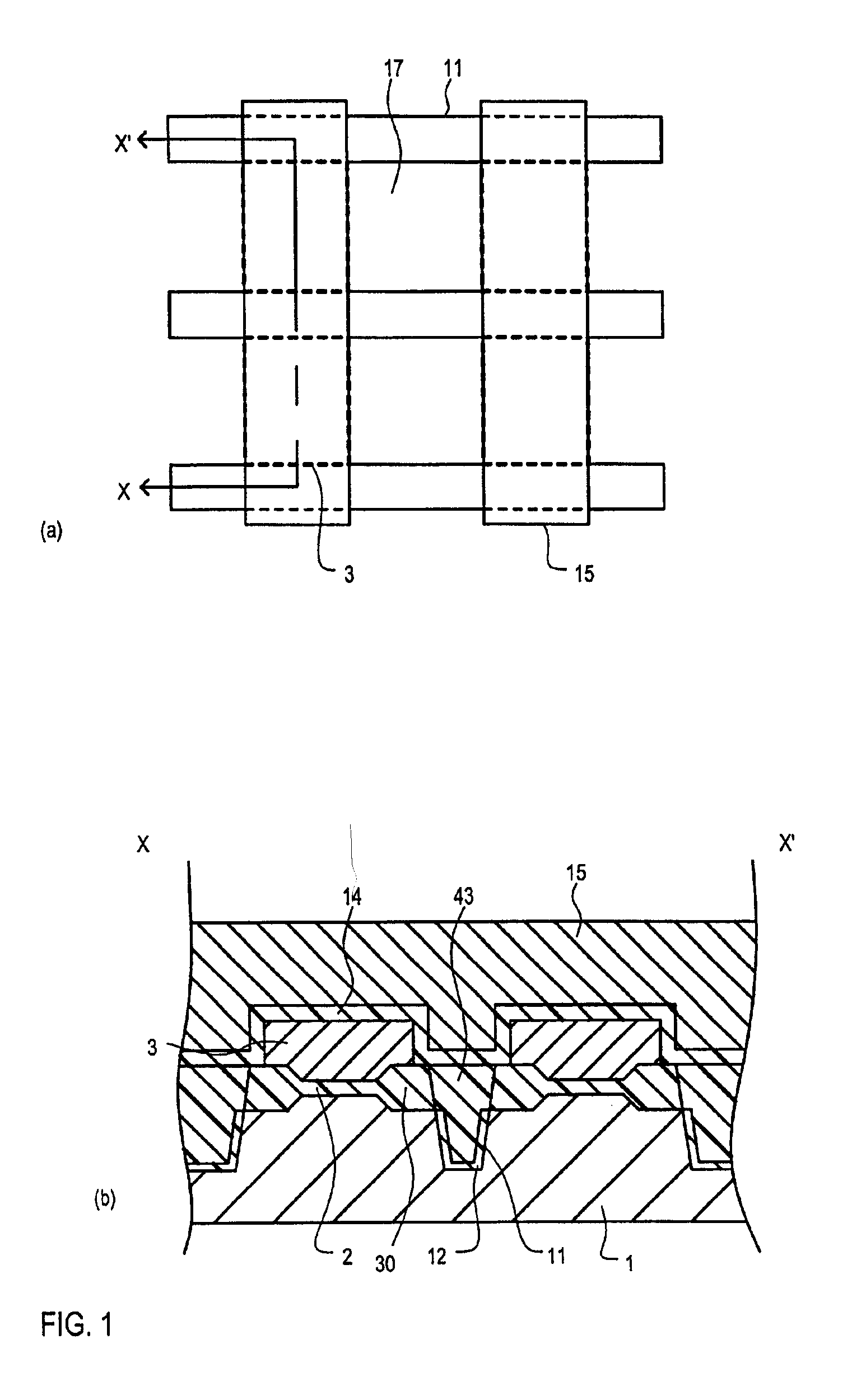
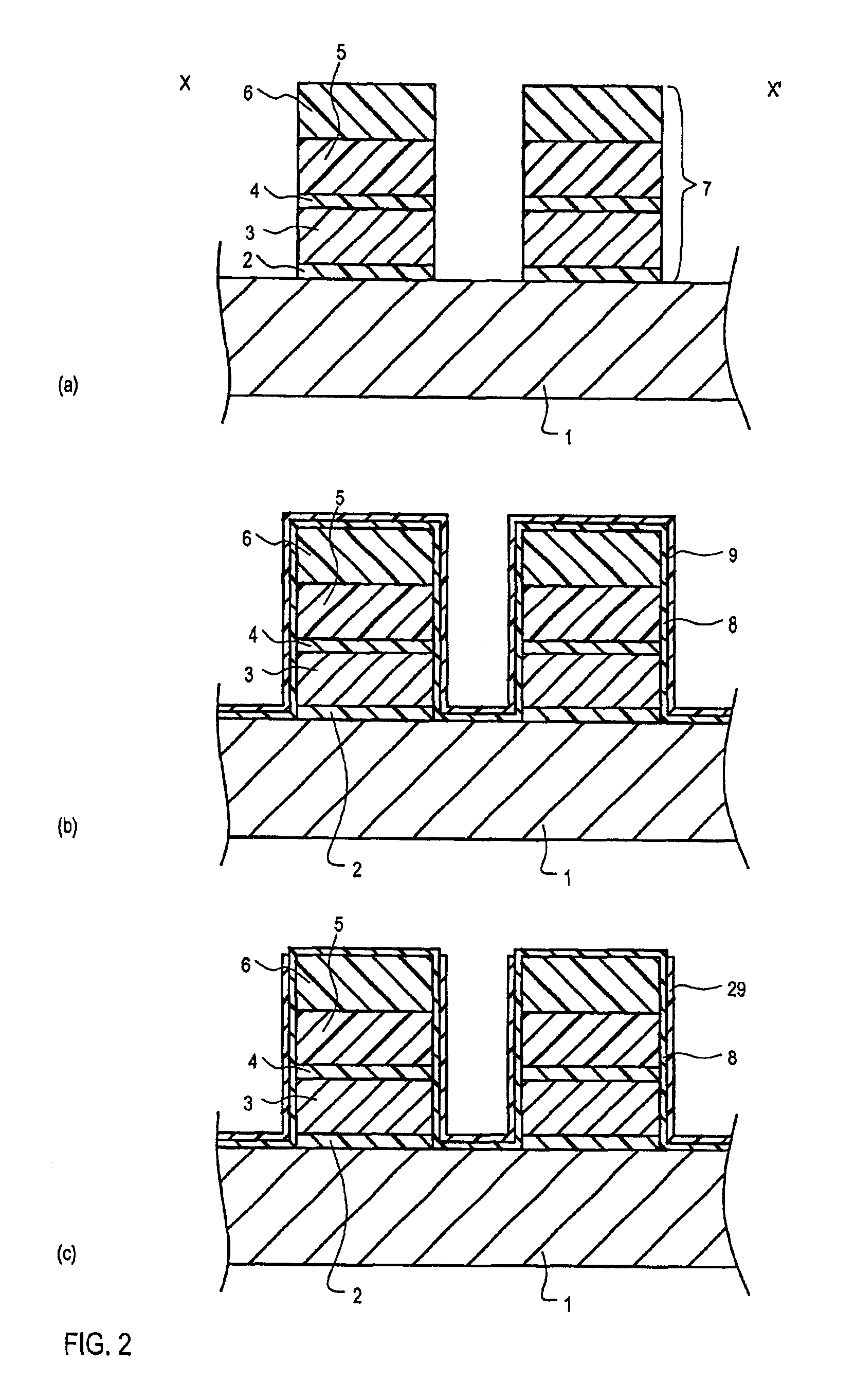
the present invention will now be described with reference to FIG. 1. FIG. 1(a) is a plan view illustrating regions including a diffusion layer and shallow trench isolation (STI) of a semiconductor device in accordance with the first embodiment. The plan view of FIG. 1(a) may be of a group of flash memory cells. FIG. 1(b) is a cross-sectional view of the semiconductor device after various processing steps in accordance with the first embodiment. FIG. 1(b) may be a cross-sectional view taken along line X—X′ as illustrated in FIG. 1(a).

As illustrated in FIGS. 1(a) and 1(b), a flash memory cell structure on a semiconductor substrate 1 may include a tunnel oxide film 2 in the vicinity of a center directly below a floating gate electrode 3. A gate oxide film 30 may be in the vicinity of the edge of the floating gate electrode 3. Gate oxide film 30 may have a thickness that is greater than the thickness of tunnel oxide film 2. The flash memory cell structure may include a shallow trench i...

second embodiment

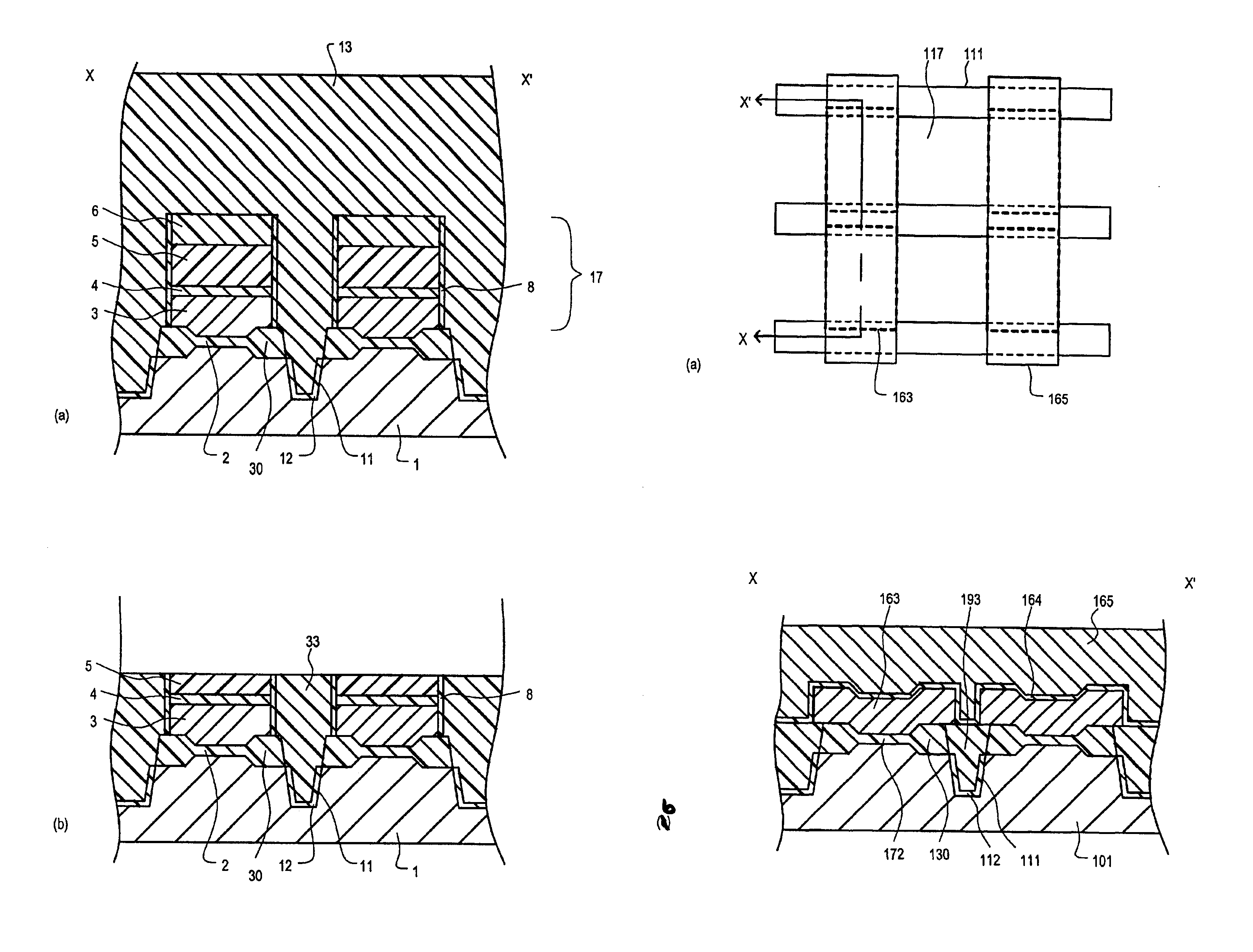
the present invention will now be described with reference to FIGS. 6 to 10. FIG. 6(a) is a plan view illustrating regions including a diffusion layer and shallow trench isolation (STI) of a semiconductor device in accordance with the second embodiment. The plan view of FIG. 6(a) may be of a group of flash memory cells. FIG. 6(b) is a cross-sectional view of the semiconductor device after various processing steps in accordance with the second embodiment. FIG. 6(b) may be a cross-sectional view taken along line X—X′ as illustrated in FIG. 6(a).

The present embodiment may include a feature in that a capacitance ratio of a control capacitance compared to a substrate capacitance may be higher than that of the first embodiment. This may be accomplished by forming a floating gate electrode having a recess shape. Otherwise, the basic structure may be similar to that of the first embodiment.

As illustrated in FIGS. 6(a) and 6(b), a flash memory cell structure on a semiconductor substrate 101 ...

third embodiment

the present invention will now be described with reference to FIGS. 11 to 15. FIG. 11(a) is a plan view illustrating regions including a diffusion layer and shallow trench isolation (STD of a semiconductor device in accordance with the third embodiment. The plan view of FIG. 11(a) may be of a group of flash memory cells. FIG. 11(b) is a cross-sectional view of the semiconductor device after various processing steps in accordance with the third embodiment. FIG. 11(b) may be a cross-sectional view taken along line X—X′ as illustrated in FIG. 11(a).

The present embodiment may include a feature in that the manufacturing process may be further simplified in comparison to the first and second embodiments while maintaining the basic structure of the first embodiment. Because the manufacturing method of the present embodiment may be identical to the manufacturing method up to the flash memory cell structure as illustrated in FIG. 8(c) of the second embodiment, only later steps may be describ...


PUM


Abstract

A semiconductor device including memory cells isolated by a trench that may be self aligned with a stacked film pattern (7) has been disclosed. The memory cells may be flash memory cells having an active gate film (2) that may be thinner than a gate oxide film (30). The active gate film (2) may be located in a central portion under of a gate electrode (3). The gate oxide film (30) may be located under end portions of the gate electrode (3). In this way, a distance between a shoulder portion of a trench (11) and a gate electrode (3) may be increased. Thus, an electric field concentration in the shoulder portion of the trench (11) may be decreased and memory cell characteristics may be improved.

Description

TECHNICAL FIELDThe present invention relates generally to a semiconductor device and its manufacturing method and more particularly to a semiconductor device having element isolation using a trench that can be self-aligned with a stacked film pattern formed in a cell.BACKGROUND OF THE INVENTIONA flash memory cell using a method in which a trench that is self-aligned with a stacked film pattern formed in the memory cell is used in element isolation has advantages that allow the distance between adjacent memory cells to be minimized so that the memory cells can be more densely arranged.Such a method is disclosed in Japanese Patent Application 11-26731 (JPA 11-26731) and is illustrated in FIG. 14. FIGS. 14(a)-(c) are cross sections of a conventional semiconductor device after various processing steps.Referring now to FIG. 14(a), a stacked film of a tunnel oxide film 204, a first floating gate electrode 203, and a nitride film 205 is formed on a semiconductor substrate 201. A trench 211...

Claims


Application Information

Patent Timeline
Patent Type & Authority Patents(United States)
IPC IPC(8): H01L21/762H01L21/70H01L27/115H01L21/8247H01L21/76H01L29/788H01L29/792
CPCH01L21/76202H01L27/11521H01L27/115H01L21/76224H10B69/00H10B41/30H01L21/76
Inventor KANAMORI, KOHJI
Owner RENESAS ELECTRONICS CORP
Why Eureka
Try Eureka