

High-power LGA socket
a high-power, lga socket technology, applied in the direction of coupling device connection, coupling contact member, coupling/disassembly of coupling parts, etc., can solve the problems of device input/output elements that are required, and limited current carrying capacity of land grid array packages
- Summary
- Abstract
- Description
- Claims
- Application Information
AI Technical Summary
Benefits of technology
Problems solved by technology
Method used
Image

Examples
Embodiment Construction
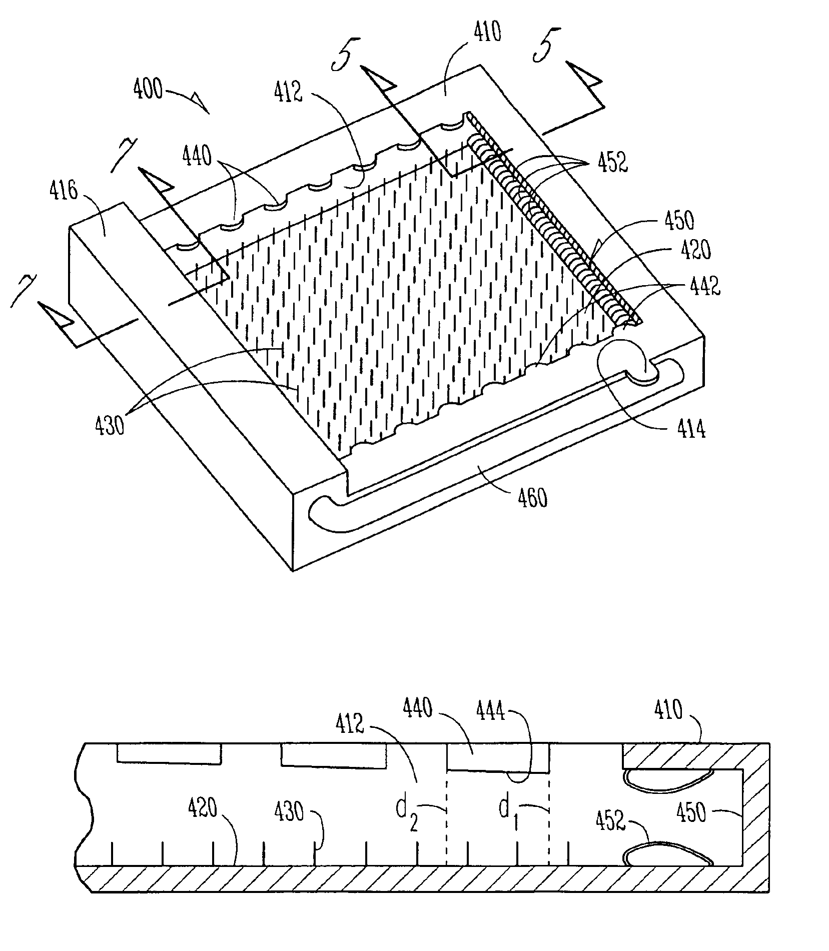
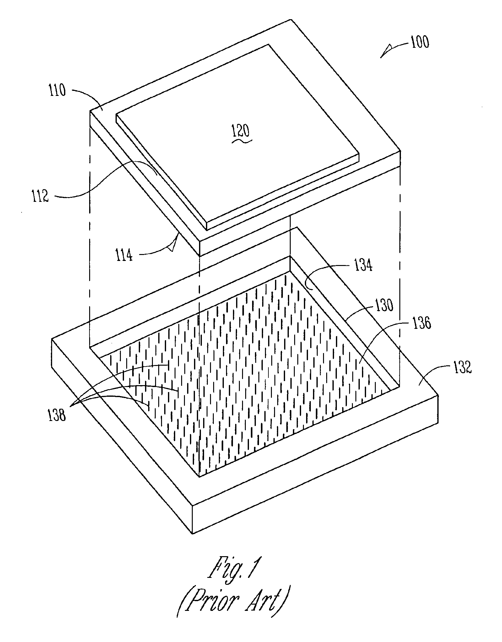
FIG. 1 illustrates a perspective top view of a prior art land grid array type package 100. The land grid array package includes a substrate 110 to which a die 120 is attached. The substrate includes a first major surface 112 and a second major surface 114. The die 120 is attached to the first major surface 112 of the substrate 110. Located on the second major surface 114 of the substrate 110 is an array of lands. The lands carry both input / output signals to and from the electronics located within the die 120, as well as the current for power as required by the electronics within the die 120. Thus, the land grid array type package 100 of the prior art has the land carrying both the currents necessary for power, as well as the signal level currents for input and output to the electronics within the die 120. The die 120 fits within a corresponding socket 130 that includes a base 132 having an opening 134 therein. At the bottom of the opening 134 is a major surface 136, which includes a...
PUM
| Property | Measurement | Unit |
|---|---|---|
| Electrical conductivity | aaaaa | aaaaa |
| Current | aaaaa | aaaaa |
| Distance | aaaaa | aaaaa |
Abstract
Description
Claims
Application Information