Flip clip attach and copper clip attach on MOSFET device

Inactive Publication Date: 2005-03-22
SEMICON COMPONENTS IND LLC
View PDF33 Cites 56 Cited by
  • Summary
  • Abstract
  • Description
  • Claims
  • Application Information

AI Technical Summary

Benefits of technology

Thus, the present invention provides an improved chip device and a method of making it. The process does not require any wire bonding because the drain connections are directly soldered on the copper clip during solder reflow while the source and gate bumps are directly coupled to the leadframe. The resulting gate connections are more reliable compared to those produced by the gate

Problems solved by technology

When gold wire bonding is done on a gate connection within a chip, the use of adhesives will introduce resin bleeds that are difficult to control and can interfere with the gate bond contact integrity.
When silver-filled adhesives are used on the source and drain connections, since adhesives do not flow selectively, the resulting device is

Method used


Image

  • Flip clip attach and copper clip attach on MOSFET device
  • Flip clip attach and copper clip attach on MOSFET device
  • Flip clip attach and copper clip attach on MOSFET device

Examples


Example

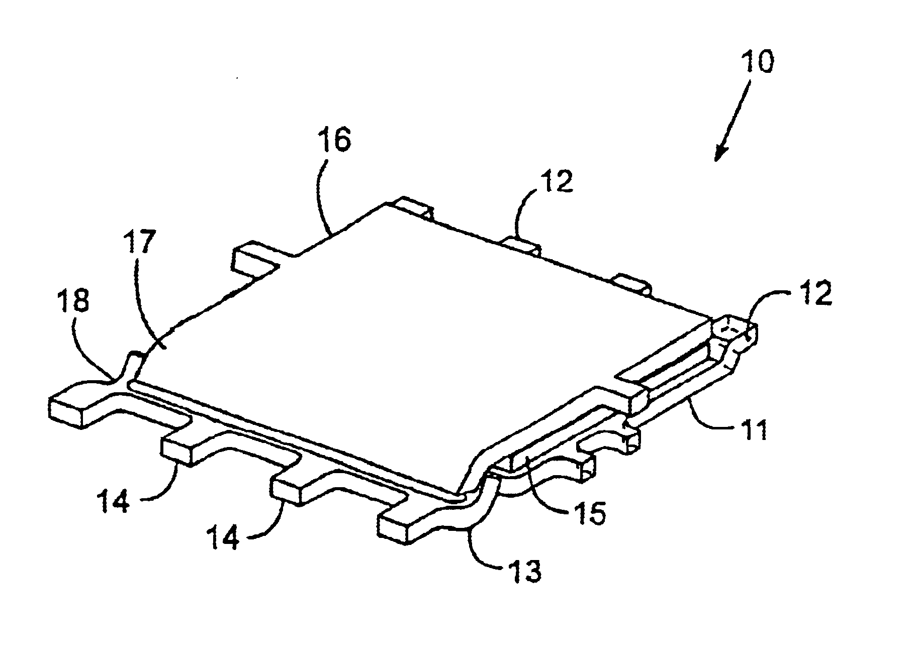
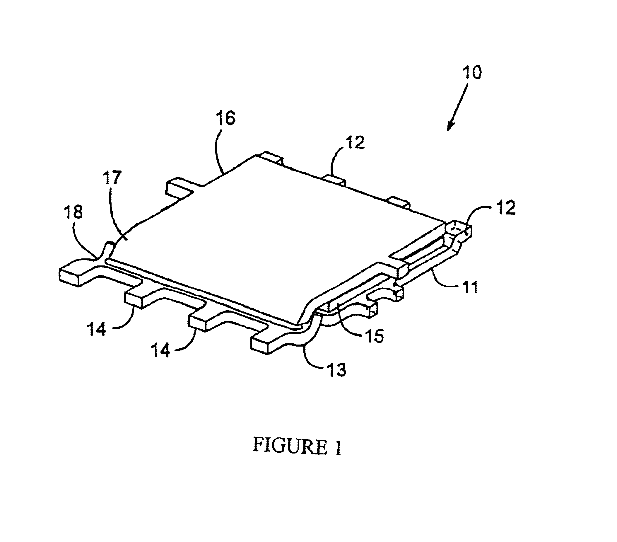
FIG. 1 illustrates a chip device 10 in accordance with the present invention. The chip device includes a leadframe 11 that includes a plurality of leads 12 and a separate lead rail 13 that includes a plurality of leads 14. A bumped die 15 is attached to the leadframe. A clip 16 is placed on the bumped die backside and attached thereto. Additionally, an edge 17 of the clip is placed within a v-groove 18 of the lead rail.

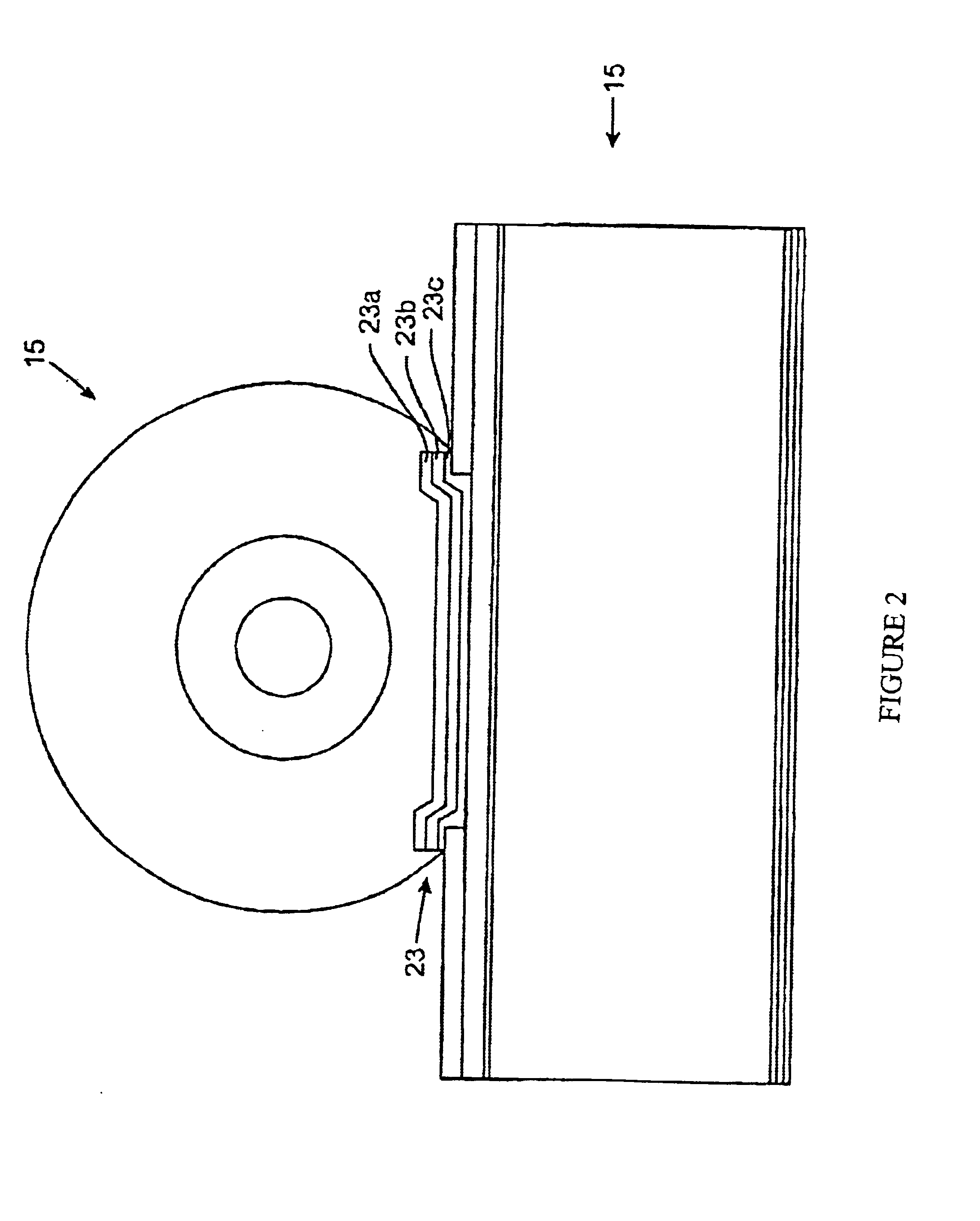
As can be seen in FIG. 4, bumped die 15 includes a plurality of solder bumps 20, preferably arranged in rows over a source area 21 of the die on a top surface of the die. A solder bump 22 is also placed on a gate area 20g of the die, which is also on the top surface of the die.

Preferably, the bumped die is provided as a single unit.

Die 15 is preferably a one-piece item that is often referred to in the art as a “bumped die” As can be seen in FIG. 2, a bumped die includes a die an “under bump material” that serves as an intermediate layer 26 between the top surface of t...


PUM


Abstract

A chip device including a leadframe that includes source and gate connections, a bumped die including solder bumps on a top side that is attached to the leadframe such that the solder bumps contact the source and gate connections, and a copper clip attached to the backside of the bumped die such that the copper clip contacts drain regions of the bumped die and a lead rail. The chip device is manufactured by flip chipping a bumped die onto the leadframe and placing the copper clip on a backside of; the trench die such that the backside of the trench die is coupled to the lead rail. The process involves reflowing the solder bumps on the bumped die and solder paste that is placed between the copper clip and the backside of the bumped die.

Description

BACKGROUND OF THE INVENTION1. Field of the InventionThe present invention relates to a chip device and a method of manufacture thereof and more particularly, to a chip device and a method of manufacture thereof that includes direct attachment of a bumped die to a leadframe and coupling of a set of leads to the bump die with a clip.2. Description of the Prior ArtSemiconductor power switching devices, and particularly, power MOSFET devices continue to push the lower limits of on-state resistance. While silicon technology has advanced significantly in the past decade, essentially the same decades old package technology continues as the primary packaging means. The epoxy or soldered die attach along with aluminum or gold wire interconnects is still a preferred power device package methodology.Recently, chip devices have been manufactured and packaged by connecting the die within the device to the leads directly through a low resistance solder connection. By using a second leadframe elem...

Claims


Application Information

Patent Timeline
IPC IPC(8): H01L23/495H01L23/48H01L21/60
CPCH01L23/49562H01L24/34H01L2224/37147H01L2924/01004H01L2924/01013H01L2924/01029H01L2924/01046H01L2924/01078H01L2924/01079H01L2924/01082H01L2924/01023H01L2924/01033H01L2924/01047H01L2924/13091H01L2924/00H01L2224/40245H01L2224/45144H01L24/37H01L24/40H01L2224/84801H01L2224/16245H01L24/84H01L2224/81801H01L24/81H01L2924/00014H01L2224/73221
Inventor ESTACIO, MARIA CRISTINA B.QUINONES, MARIA CLEMENS Y.
Owner SEMICON COMPONENTS IND LLC
Why Eureka
Try Eureka