Method and apparatus to attenuate power plane noise on a printed circuit board using high ESR capacitors

a technology of capacitors and printed circuit boards, applied in the field of electronic circuits, can solve the problems of affecting the normal operation of circuitry, and the generation of relatively large amplitude emi, and achieve the effect of reducing or minimizing the noise of printed circuit boards

Inactive Publication Date: 2005-03-22
HEWLETT-PACKARD ENTERPRISE DEV LP +1
View PDF9 Cites 34 Cited by
  • Summary
  • Abstract
  • Description
  • Claims
  • Application Information

AI Technical Summary

Benefits of technology

In another embodiment of the invention, the simulation is performed over a range of bypass capacitor values and over a range of frequency values. In yet another embodiment of the invention, the model of the printed circuit board includes a model of

Problems solved by technology

If the amplitude of the EMI is high enough, it may disrupt normal operations of circuitry.
Printed circuit boards (PCBs), to which integrated circuits are coupled, can generate relatively large amplitude EMI.
These simultaneous current fluctuations from the power plane or onto the ground plane can cumulatively create large amplitude EMI emissions.
If this noise is too large, it may cause an error in the integrated circuit which will result in improper operation of an electronic device.

Method used


Image

  • Method and apparatus to attenuate power plane noise on a printed circuit board using high ESR capacitors
  • Method and apparatus to attenuate power plane noise on a printed circuit board using high ESR capacitors
  • Method and apparatus to attenuate power plane noise on a printed circuit board using high ESR capacitors

Examples


Embodiment Construction

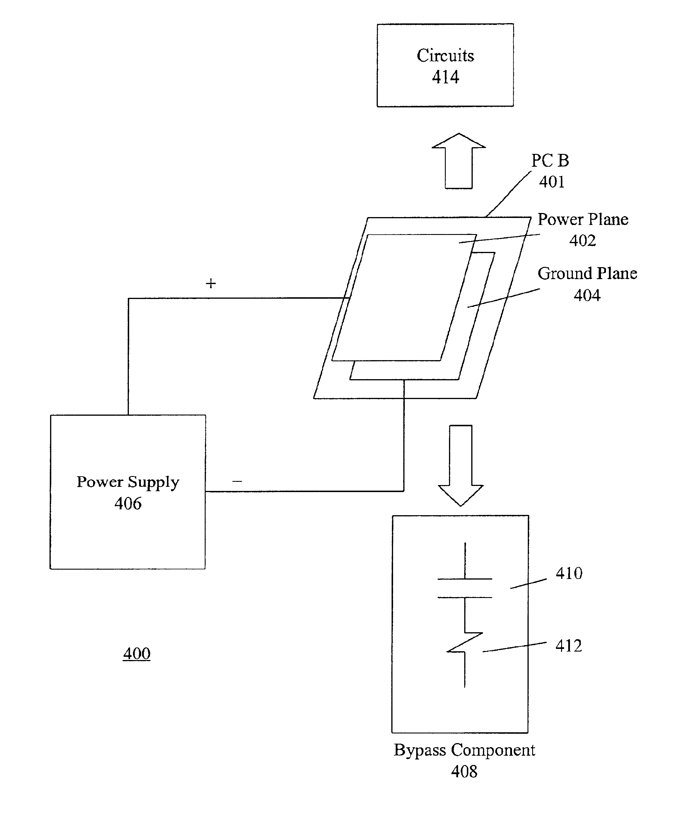
Designing high-speed digital systems to meet noise, electromagnetic interference (EMI), radio frequency interference (RFI), and Federal Communications Commission (FCC) requirements is a challenge that starts with the layout of a printed circuit board (PCB), also called a printed wiring board (PWB). To avoid multiple design iterations and costly end-product noise or EMI “fixes,” the printed circuit board design process has to generate boards that meet both signal integrity and radiated emissions criteria.

Today's higher clock frequencies and faster rise times often cause traces on PCBs to act like antennas thereby increasing undesirable EMI and RFI emissions. High speed (e.g., pico-second) edge times also result in high-speed performance problems such as cross talk, ringing, overshoot, undershoot, and ground bounce.

Thus, it has been observed that sound design techniques at the PCB level according to the present invention results in improved signal integrity (e.g., reduced power distri...


PUM


Abstract

In a method of the present invention, performance characteristics of a printed circuit board are analyzed. The printed circuit board, bypass components and an applied stimulus are modeled. Each of the bypass components includes a capacitor and a resistor in series with each other. Alternatively, a second capacitor is coupled in parallel to the above capacitor and resistor. A simulation of the circuit model is then performed. In this embodiment of the invention, the simulation is responsive to the stimulus as is performed over a range of bypass resistor values. In another embodiment of the invention, a printed circuit board is described with components and characteristics that reduce noise. Such a printed circuit board includes a power plane and a plurality of bypass components. Moreover, the plurality of bypass components include bypass capacitors and bypass resistors coupled in series between the positive power plane and the negative power plane.

Description

FIELD OF THE INVENTIONThe present invention relates to the field of electronic circuits. More particularly, the present invention relates to printed circuit boards and methods for reducing power plane noise on such printed circuit boards.BACKGROUND OF THE INVENTIONA wide variety of electrical components have become part of everyday life. In a typical day, a person may use an alarm clock, a computer, a television, and countless other electrically powered tools and appliances. The electric current used to operate each of these components produces both electric fields and magnetic fields, collectively referred to herein as electromagnetic (EM) fields.As current passes through a conductor, the conductor acts like an antenna to transmit EM fields into the surrounding environment, much like a radio transmission antenna. Conversely, when a conductor is placed in an EM field, current is generated in the conductor, much like a radio reception antenna. So, the EM fields emitted by one electri...

Claims


Application Information

Patent Timeline
IPC IPC(8): G06F17/50H05K9/00H05K1/02H05K3/00
CPCG06F17/5036H05K9/0039H05K1/0234H05K1/0231H05K2201/09309H05K3/0005G06F30/367
Inventor GREBENKEMPER, JOHN
Owner HEWLETT-PACKARD ENTERPRISE DEV LP
Why Eureka
Try Eureka