Semiconductor slider with an integral spin valve transistor structure and method for making same without a bonding step

a semiconductor slider and transistor technology, applied in nanoinformatics, instruments, record information storage, etc., can solve the problems of not having a method known in the art for fabricating a slider incorporating an integral svt and other electronic components in a conventional thin-film process, and achieves the effects of improving the sensitivity of the svt to external magnetic fields, reducing the barrier height, and increasing the hot electron injection level on the substra

Inactive Publication Date: 2005-03-22
HITACHI GLOBAL STORAGE TECH NETHERLANDS BV
View PDF24 Cites 21 Cited by
  • Summary
  • Abstract
  • Description
  • Claims
  • Application Information

AI Technical Summary

Benefits of technology

[0016]It is an advantage of this invention that SVT sensor side-reading may be limited with standard processing steps during slider fabrication. It is a feature of the method of this invention that an over-etching step may be employed to leave the SVT base region isolated on a semiconductor pedestal, which may then be covered with FM shield material to minimize sensitivity to magnetic fields at the sides. Such a procedure may provide RW of less than 250 nm.

Problems solved by technology

Until now, there was no method known in the art for fabricating a slider incorporating an integral SVT and other electronic components in a conventional thin-film process.

Method used


Image

  • Semiconductor slider with an integral spin valve transistor structure and method for making same without a bonding step
  • Semiconductor slider with an integral spin valve transistor structure and method for making same without a bonding step
  • Semiconductor slider with an integral spin valve transistor structure and method for making same without a bonding step

Examples


Embodiment Construction

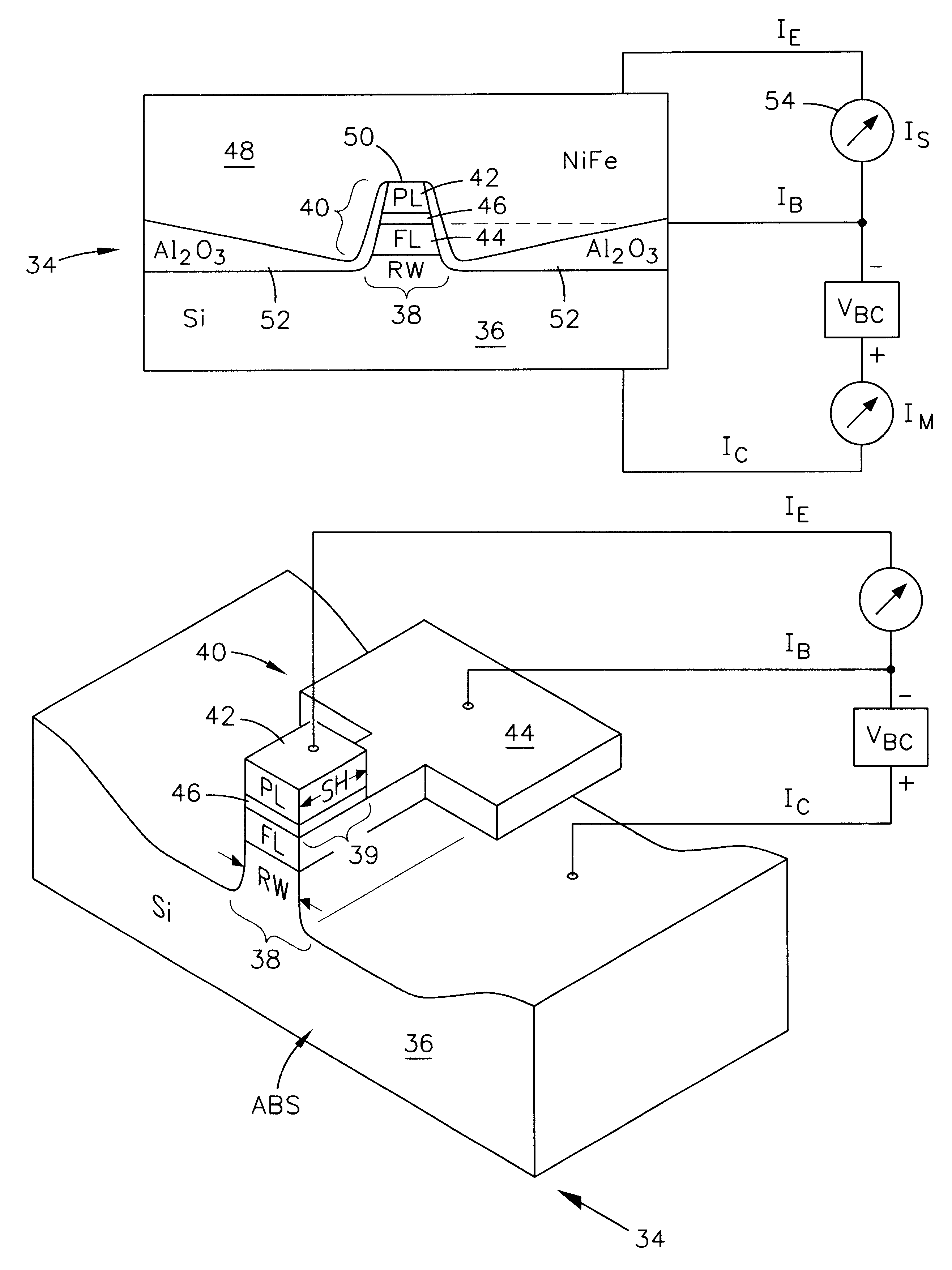
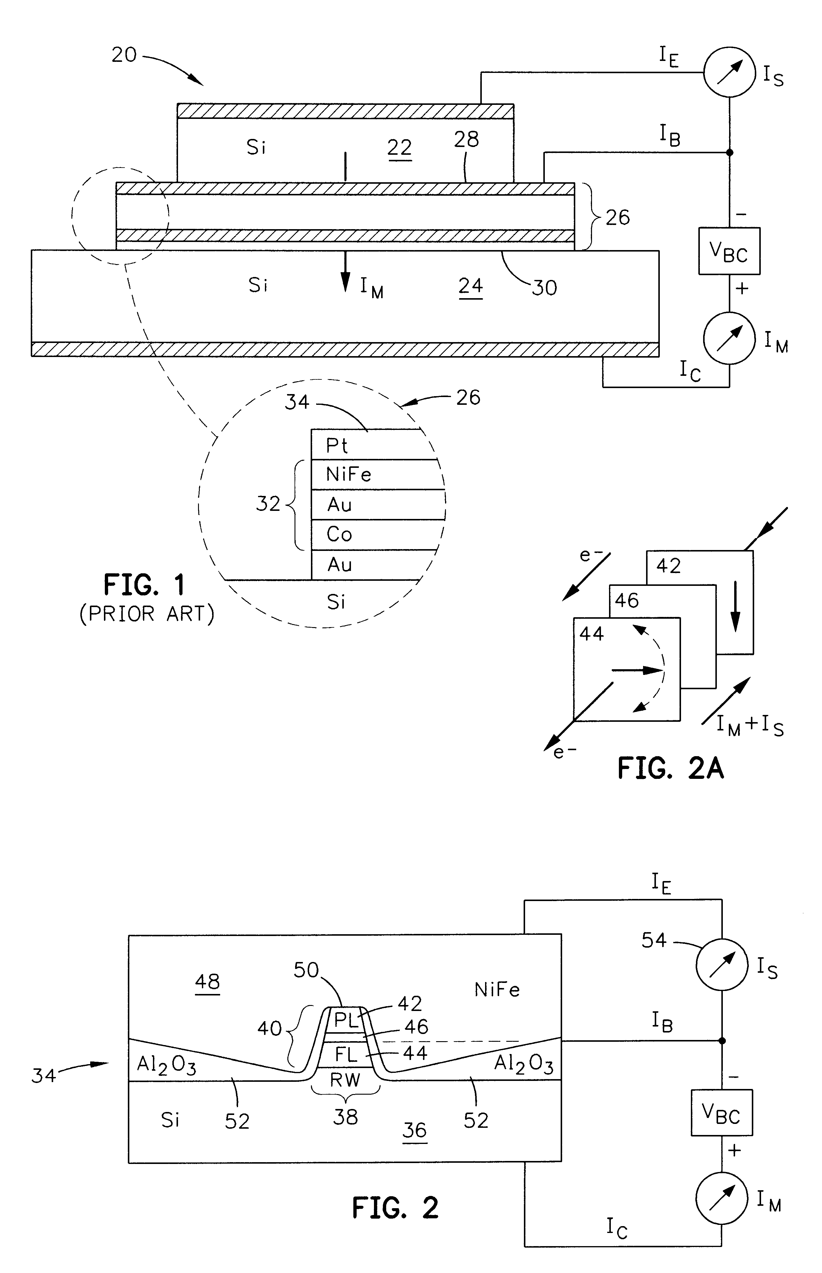
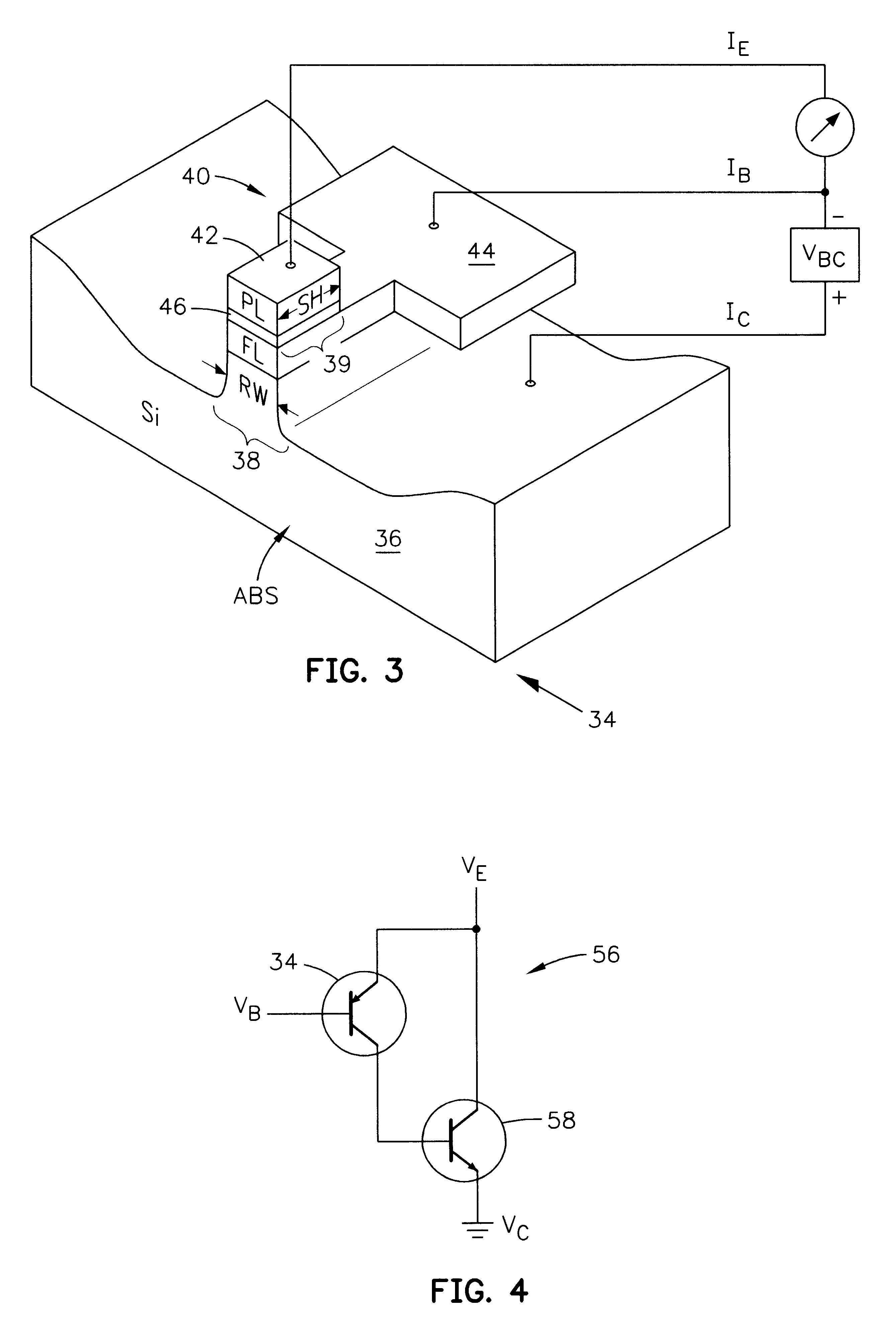
[0044]FIG. 2 (not to scale) illustrates a portion of the air-bearing surface (ABS) of the slider of this invention, limited to the ABS view of the integral spin valve transistor (SVT) 34 of this invention. The monolithic wafer semiconductor collector layer 36 carries the collector current IC of SVT 34 and supports a semiconductor pedestal 38. The width of semiconductor pedestal 38 generally defines the read width (RW) of SVT 34, which may be 250 nm, for example. Semiconductor pedestal 38 supports a sensor stack 40, which has a similar width RW over a depth defined by the stripe height (SH) 39 as shown. Sensor stack 40 may have a total thickness of 50 nm, for example, and may, for example, include a spin valve (SV) stack including a FM pinned layer structure 42 separated from a FM free layer 44 by the conductive nonmagnetic spacer layer 46. FIG. 2 is not to scale and spacer layer 46 may consist of a 2.0 nm layer of copper, for example. Alternatively, sensor stack 40 may, for example,...


PUM

PropertyMeasurementUnit
coercivityaaaaaaaaaa
read widthaaaaaaaaaa
temperaturesaaaaaaaaaa

Abstract

A semiconductor slider including an integral spin valve transistor (SVT) having a read width of 250 nm or less disposed on a monolithic semiconductor substrate, useful in magnetic data storage applications. The monolithic slider may also include other magnetic and semiconductor transistor structures and is fabricated in a single process using standard thin-film processing steps. The SVT includes a sensor stack having a top surface and including a first ferromagnetic (FM) layer in contact with and forming a Schottky barrier at the monolithic semiconductor substrate, a FM shield layer disposed over the sensor stack and in electrical contact with the top surface thereof, a SVT emitter terminal coupled to the FM shield, a SVT collector terminal coupled to the substrate and a SVT base terminal coupled to the first FM layer. The sensor stack may include a spin valve (SV) stack or a tunnel valve (TV) stack, for example.

Description

BACKGROUND OF THE INVENTION[0002]1. Field of the Invention[0003]This invention relates generally to spin valve transistor structures for magnetic read heads and more particularly to an integral spin valve transistor (SVT) structure formed in a semiconductor slider without the usual SVT wafer bonding step.[0004]2. Description of the Related Art[0005]Magneto-electronic devices with improved magnetic sensitivity are vital to increasing magnetic data storage densities. Giant magnetoresistance (GMR) sensors using only two layers of ferromagnetic (FM) material, the free (sensing) layer and the pinned (reference) layer, separated by a layer of non-magnetic conductive material (e.g., copper) are generally referred to as spin valve (SV) sensors and represent a major improvement that relies on the spin-dependent scattering effect. In SV sensors, the resistance of a spin valve (SV) to a sense current varies as a function of the spin-dependent transmission of the conduction electrons between tw...

Claims


Application Information

Patent Timeline
Patent Type & Authority Patents(United States)
IPC IPC(8): G11B5/33G11B5/10G11B5/39G11B5/31
CPCB82Y10/00G11B5/332G11B5/102G11B5/3103G11B5/3967G11B5/3903G11B5/3163
Inventor CHILDRESS, JEFFREY ROBINSONFONTANA, JR., ROBERT EDWARDLILLE, JEFFREY S.
Owner HITACHI GLOBAL STORAGE TECH NETHERLANDS BV
Why Eureka
Try Eureka