Method for detecting the endpoint of a chemical mechanical polishing (CMP) process

a technology of mechanical polishing and endpoint detection, which is applied in the direction of manufacturing tools, grinding machine components, lapping machines, etc., can solve the problems of mechanical and chemical polishing effects on the wafer, and achieve the effect of accurately varying the temperature of the polishing pad and eliminating interferen

Inactive Publication Date: 2005-03-29
NATIONAL TSING HUA UNIVERSITY
View PDF8 Cites 10 Cited by
  • Summary
  • Abstract
  • Description
  • Claims
  • Application Information

AI Technical Summary

Benefits of technology

The difference between the measured polishing pad and the environmental temperature is calculated to obtain a raised temperature difference of the polishing pad for polishing, in order to get the variation of the polishing pad temperature accurately and to eliminate the interference from the polishing slurry to said non-contact measuring device.

Problems solved by technology

It causes mechanical and chemical polishing effects to the wafer between the carrier and the polishing pad.

Method used


Image

  • Method for detecting the endpoint of a chemical mechanical polishing (CMP) process
  • Method for detecting the endpoint of a chemical mechanical polishing (CMP) process
  • Method for detecting the endpoint of a chemical mechanical polishing (CMP) process

Examples


Embodiment Construction

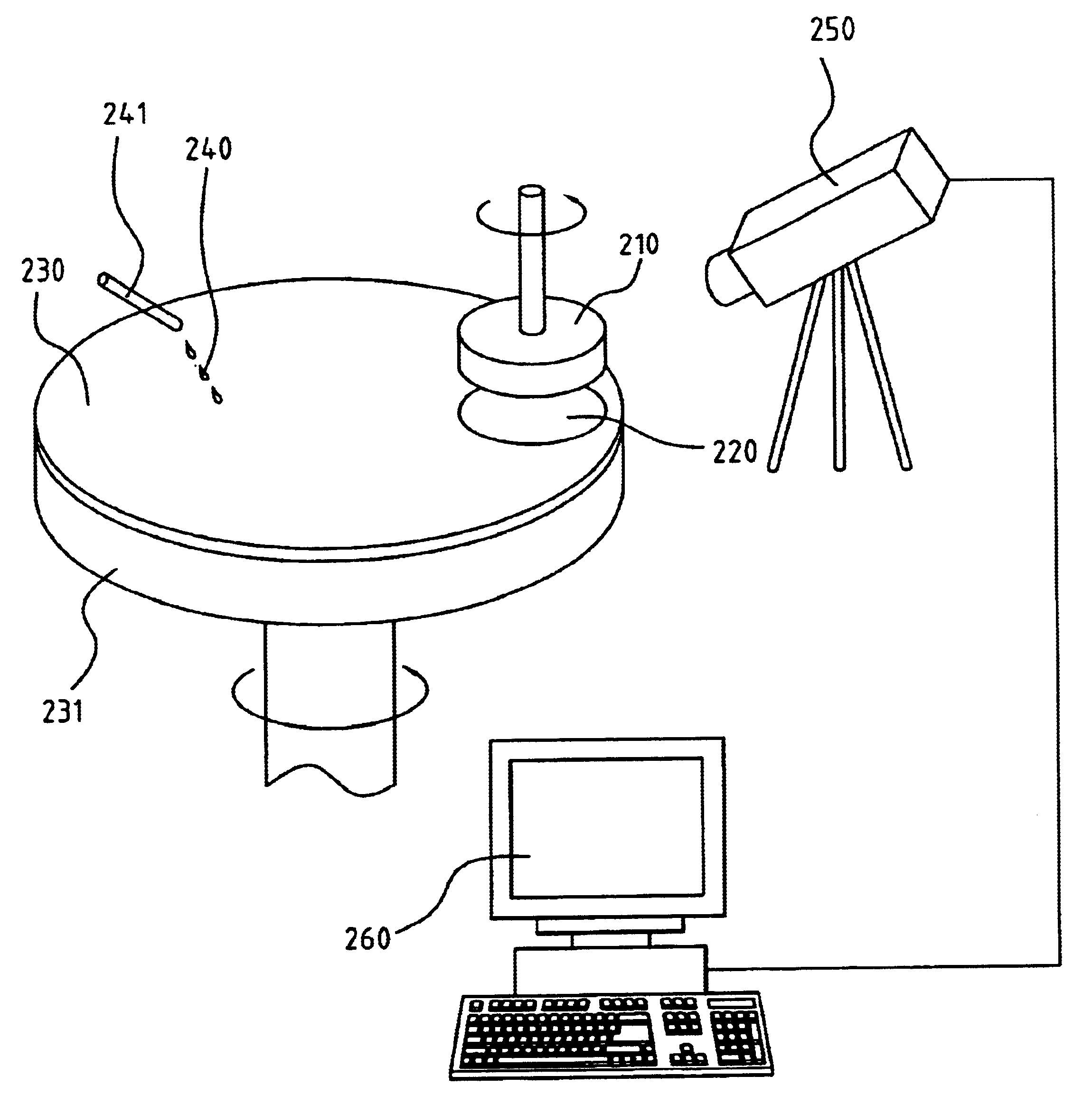
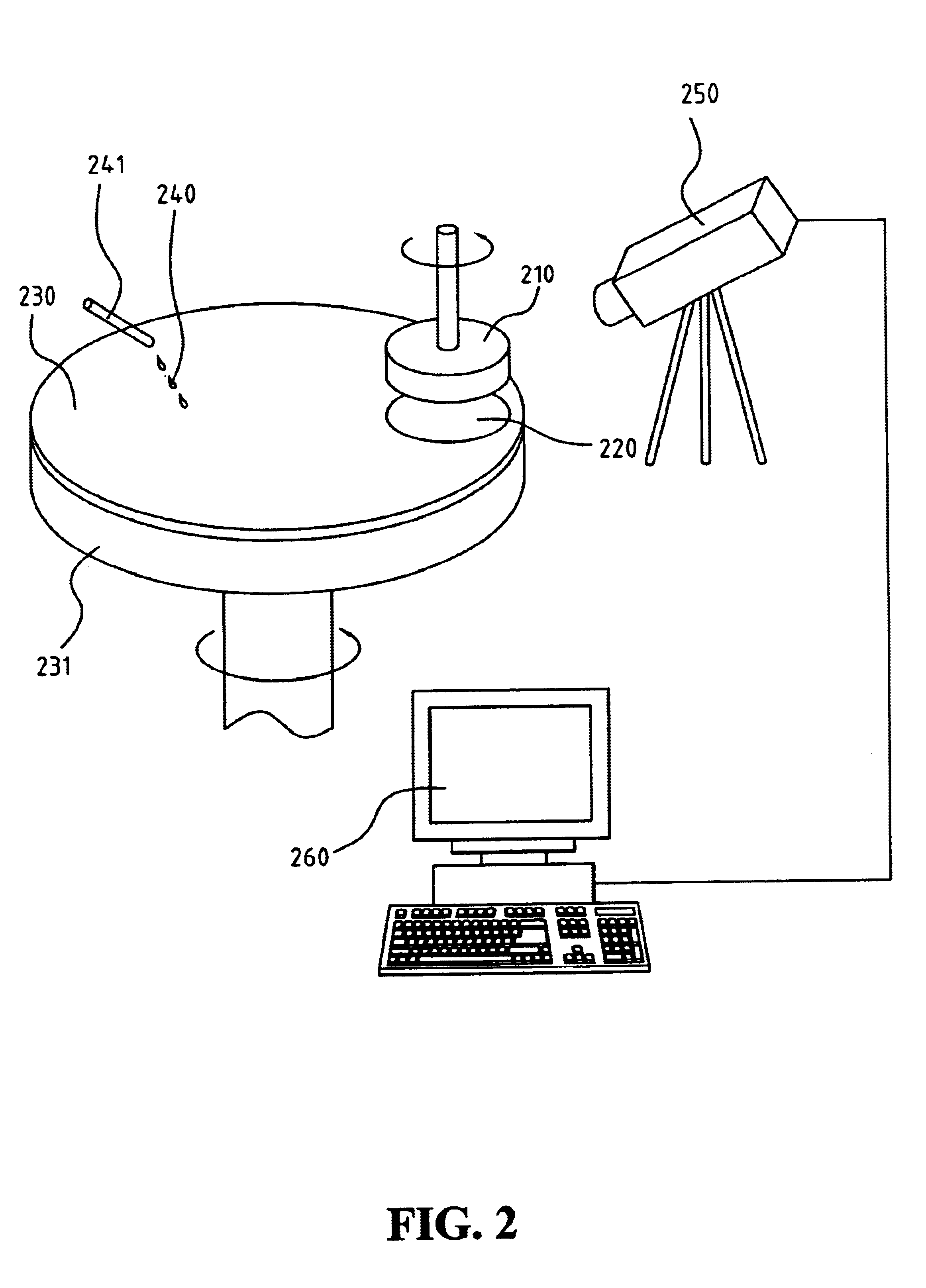
FIG. 2 shows the apparatus according to the present invention. With reference to FIG. 2, the CMP apparatus of the invention includes a carrier 210, for holding a semiconductor wafer 220. The carrier 210 fixes the wafer 220 to the surface of the polishing pad 230 attached on the rotary polishing platen 231. During planarization, the wafer 220 moves with the polishing, and polishing slurry 240 comprising an abrasive fluid, such as silica or alumina abrasive particles suspended in either a basic or an acidic solution, is dispended on the pad and flows into the gap between the wafer 220 and the polishing pad 230, through a conduit 241 above the polishing pad 230. Mechanical and chemical polishing effects take place on the wafer 220. The combination of mechanical and chemical polishing effects makes the removal of the excessive metal material from the surface of the wafer 220, and thus planarizes the wafer 220. Furthermore, a non-contact thermal image camera 250 linked to a PC 260 is set...


PUM


Abstract

A method for detecting the endpoint of a chemical mechanical polishing (CMP) process uses the slope variation of temperature difference of polishing pad. The method combines temperature measurement at polishing pad and atmosphere, and numerical analysis to figure out the curve of temperature difference variation versus polishing time. The endpoint of CMP is determined by the change of the slope of the curve. The method allows endpoint to be detected in-situ at the polishing apparatus, without stopping polishing process.

Description

FIELD OF THE INVENTIONThe present invention relates to a semiconductor manufacturing process, and more particularly to a method to detect the endpoint of a chemical mechanical polishing (CMP) process based on the temperature slope of the polishing pad.BACKGROUND OF THE INVENTIONAdvances in semiconductor manufacturing technology have enabled progress to be seen in the scale finely. In the semiconductor manufacturing of a deep submicron process, the depth of focus shrinks constantly to reach the need for increasing speed and the resolution for lithography raises constantly as well. In order to accomplish the above purposes, global planarization of the wafer surface is highly required, and therefore a CMP process to achieve the goal is also needed.FIG. 1 shows a conventional CMP apparatus. With reference to FIG. 1, the CMP apparatus constitutes of at least one carrier 110, for holding a semiconductor wafer 120. The carrier 110 holds the wafer 120 against the surface of the polishing pa...

Claims


Application Information

Patent Timeline
Patent Type & Authority Patents(United States)
IPC IPC(8): H01L21/02H01L21/302H01L21/461B24B37/04B24B49/12B24B49/14
CPCB24B37/013B24B49/12B24B49/14Y10S438/959Y10S438/907
Inventor HOCHENG, HONGHUANG, YUN-LIANG
Owner NATIONAL TSING HUA UNIVERSITY
Why Eureka
Try Eureka