Multi-step tungsten etchback process to preserve barrier integrity in an integrated circuit structure

a technology of integrated circuit structure and etchback process, which is applied in the direction of semiconductor/solid-state device manufacturing, basic electric elements, electric devices, etc., can solve the problem of difficult to completely remove the aluminum portion of the etching

Inactive Publication Date: 2005-03-29
INTEGRATED DEVICE TECH INC
View PDF6 Cites 13 Cited by
  • Summary
  • Abstract
  • Description
  • Claims
  • Application Information

AI Technical Summary

Problems solved by technology

However, it is difficult for the etch to entirely remove aluminum portion 51A from opening 41.

Method used


Image

  • Multi-step tungsten etchback process to preserve barrier integrity in an integrated circuit structure
  • Multi-step tungsten etchback process to preserve barrier integrity in an integrated circuit structure
  • Multi-step tungsten etchback process to preserve barrier integrity in an integrated circuit structure

Examples


Embodiment Construction

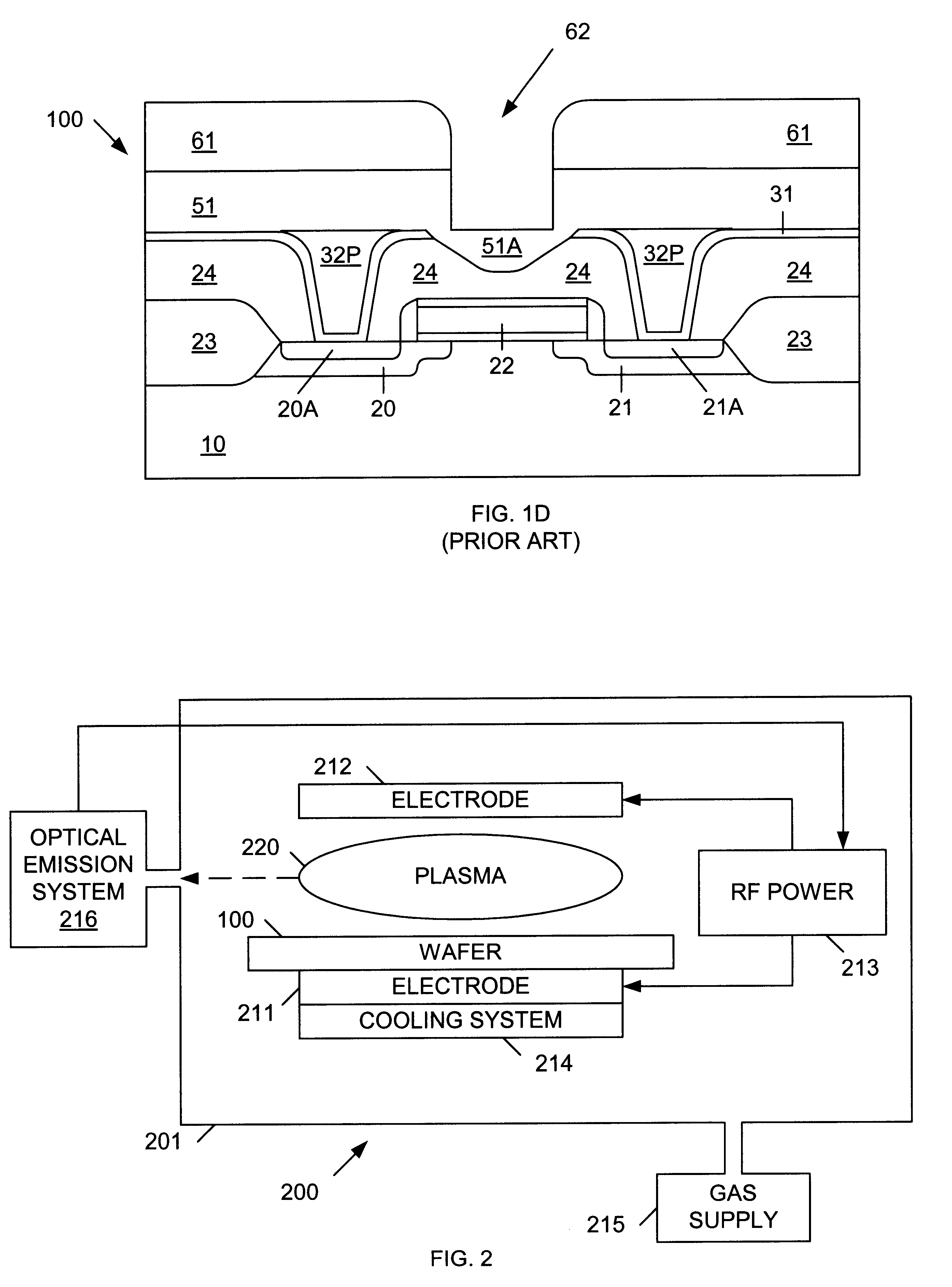
FIG. 2 is a block diagram of a semiconductor processing system 200 which is used to process the semiconductor structure 100 (FIG. 1A) in accordance with one embodiment of the present invention. System 200 includes a plasma chamber 201 which houses electrodes 211 and 212, a radio frequency (RF) power source 213, a helium cooling system 214, a gas supply system 215 and an optical emission system 216. A system including the elements of semiconductor processing system 200 can be purchased from Applied Materials.

Semiconductor structure 100 is electrostatically mounted on electrode / chuck 211. Electrode 212 is separated from electrode 211 and structure 100, with RF power source 213 providing power to electrodes 211-212. Gas supply system 215 is configured to introduce one or more gases into chamber 201. In a manner known in the art, the RF power applied to electrodes 211-212, combined with the gases introduced by gas supply system 215, results in the formation of a plasma 220 between elect...


PUM

PropertyMeasurementUnit
temperatureaaaaaaaaaa
thicknessaaaaaaaaaa
thicknessaaaaaaaaaa

Abstract

An improved method is provided for etching back a tungsten layer that overlies a titanium nitride adhesion layer on a semiconductor structure. This method includes the steps of: (1) performing a first plasma etchback of the tungsten layer for a first predetermined time period, such that a thin layer of tungsten remains over the adhesion layer at the end of the first plasma etchback, (2) actively or passively cooling the resulting semiconductor structure to a temperature of 35° C. or lower, and then (3) performing a second plasma etchback of the tungsten layer until an endpoint is detected, thereby exposing the adhesion layer. Cooling the semiconductor structure prior to the second plasma etchback ensures that the titanium nitride adhesion layer is at a relatively low temperature during the second plasma etchback. The titanium nitride adhesion layer etches significantly slower at lower temperatures, thereby making it easier to stop the second plasma etchback on the adhesion layer.

Description

BACKGROUND OF THE INVENTION1. Field of the InventionThe present invention relates to a semiconductor process for fabricating integrated circuit devices. More specifically, the present invention relates to a process used to form a tungsten plug in a contact opening or via.2. Discussion of Related ArtTungsten (W) plugs are commonly used to provide contact to the upper surfaces to active regions of circuits formed in a semiconductor wafer. To help the tungsten adhere to the semiconductor surface, an adhesion layer, such as titanium nitride (TiN) is commonly deposited before the tungsten. The adhesion layer readily adheres to the semiconductor surface, and provides a layer to which the tungsten will readily adhere.FIG. 1A is a cross-sectional view of a conventional semiconductor structure 100 that includes semiconductor substrate (wafer) 10, source region 20, drain region 21, gate structure 22 and field oxide layer 23. Regions 20A and 21A are contact regions where contact is to be made ...

Claims


Application Information

Patent Timeline
Patent Type & Authority Patents(United States)
IPC IPC(8): H01L21/02H01L21/302C23F4/00H01L21/321H01L21/3213
CPCC23F4/00H01L21/32136H01L21/32115
Inventor CAO, WANQINGLO, GUO-QIANGLEE, SHIH-KEDXUE, HONGYONG
Owner INTEGRATED DEVICE TECH INC
Why Eureka
Try Eureka