Virtual ground single transistor memory cell, memory array incorporating same, and method of operation thereof

a transistor memory cell and virtual ground technology, applied in the field of semiconductor memory, can solve the problems of adversely affecting the doping concentration and other characteristics of the bit line, and the abrupt junction, so as to simplify the scheme of counter-biasing the bit line, reduce the che generation, and enhance the che generation

Inactive Publication Date: 2005-03-29
WINBOND ELECTRONICS CORP
View PDF6 Cites 73 Cited by
  • Summary
  • Abstract
  • Description
  • Claims
  • Application Information

AI Technical Summary

Benefits of technology

Alternatively or in addition, the degree of asymmetry between the source and drain junction characteristics in the prior art may not be as great as desired, and further improvements therein can further simplify schemes for counter-biasing the bit lines.
We have developed a floating gate transistor for a memory array having enhanced CHE generation on the drain side and, in the alternative or in addition, reduced CHE generation on the source side. This structure enables less complex counter-biasing schemes to be used on the bit lines, relative to the schemes required for some conventional virtual ground architecture cell arrays.

Problems solved by technology

Unfortunately, the asymmetrical floating gate transistor of Gill uses a thermal insulator region 24 that is grown over the arsenic implant used both for the n+abrupt-junction doping and for the n+bit line doping.
The growth of the thermal insulator region 24 subsequent to the n+doping is, we believe, disadvantageous.
As the thermal oxide is grown, the arsenic implant both diffuses and is consumed by the growing oxide, which can adversely affect the doping concentration and other characteristics of the bit line and the abrupt junction.
Alternatively or in addition, the degree of asymmetry between the source and drain junction characteristics in the prior art may not be as great as desired, and further improvements therein can further simplify schemes for counter-biasing the bit lines.

Method used


Image

  • Virtual ground single transistor memory cell, memory array incorporating same, and method of operation thereof
  • Virtual ground single transistor memory cell, memory array incorporating same, and method of operation thereof
  • Virtual ground single transistor memory cell, memory array incorporating same, and method of operation thereof

Examples


Embodiment Construction

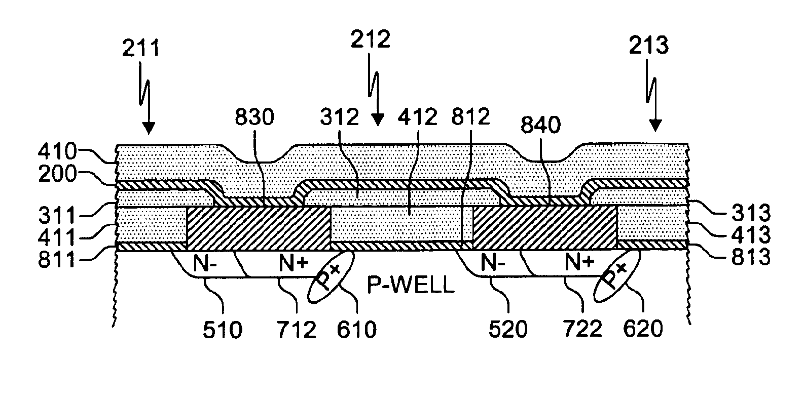
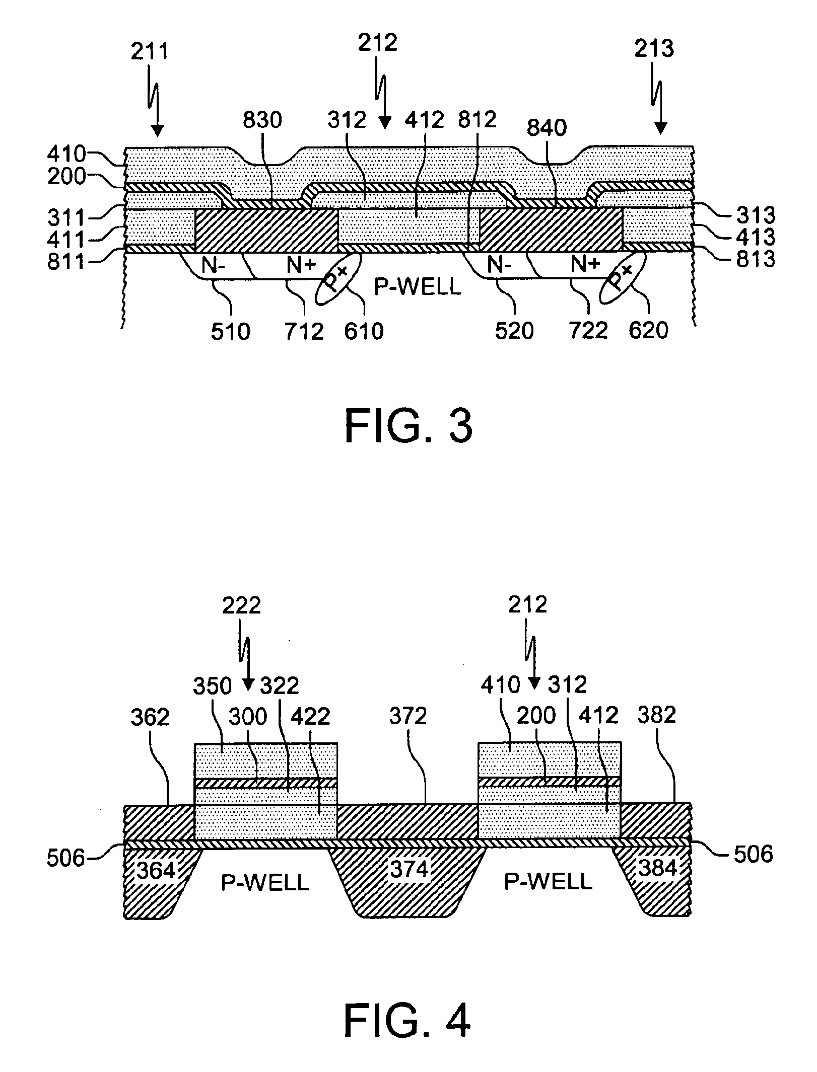
FIG. 3 is a cross-section view of three virtual ground single transistor memory cells 211, 212 and 213 that under suitable operating conditions provides enhanced CHE generation on their drain sides and suppressed CHE generation on their source sides. The transistors 211 and 213 are shown partially and the transistor 212 is shown fully. With reference to transistor 212, a control gate 410 is space from an upper section 312 of a stacked floating gate by a interpoly oxide 200. A lower section 412 of the stacked floating gate is spaced from a channel region by an ultra-thin tunnel oxide 506. The channel region is defined in a p-well on one side by a heavily doped n+ region 712 which is considered to be the drain, and on the other side by a lightly doped n− region 720 which is considered to be the source. A heavily doped p+ region 610 known as a “halo implant” is used in the channel adjacent the heavily doped n+ drain 712 to enhance the generation of channel hot electrons as well as to r...


PUM


Abstract

An asymmetrical virtual ground single transistor floating gate memory cell has a floating gate that overlies a channel region in a p-well, the channel region lying between a heavily doped n+ drain region and a lightly doped n− source region. A heavily doped p+ region known as a “halo” is disposed in the channel adjacent the heavily doped n+ drain. The floating gate is spaced away from the channel region by a generally thin tunnel oxide. A lightly doped source with a graded source/channel junction reduces source side CHE generation. In one variation, a thicker oxide between the source and the floating gate reduces CHE injection from the source side. A heavily doped drain with a halo implant in the channel adjacent the drain enhances drain side CHE generation.

Description

BACKGROUND OF THE INVENTION1. Field of the InventionThe present invention relates to semiconductor memory, and more particularly to a memory device structure for a virtual ground memory array.2. Description of the Related ArtNonvolatile memory retains stored data when power is removed, which is required or at least highly desirable in many different types of computers and other electronic devices. Nonvolatile semiconductor memory devices are generally divided into two main classes. The first class is based on the storage of charge in discrete trapping centers of a dielectric layer of the structure. The second class is based on the storage of charge on a conducting or semiconducting layer that is completely surrounded by a dielectric, typically an oxide.A common type of stored charge device is the stacked gate transistor, also known as a floating gate transistor, in which cell programming is performed through channel hot-electron injection (“CHE”). An illustrative self-aligned double...

Claims


Application Information

Patent Timeline
Patent Type & Authority Patents(United States)
IPC IPC(8): H01L21/70H01L27/115H01L21/02H01L29/66H01L21/336H01L21/8247H01L29/788G11C16/04
CPCH01L27/115H01L29/7885H01L29/66825H01L27/11521G11C16/0491H10B69/00H10B41/30
Inventor HAN, KYUNG JOONHSIA, STEVE K.PARK, JOO WEONKWON, GYU-WANLEE, JONG SEUK
Owner WINBOND ELECTRONICS CORP
Why Eureka
Try Eureka