Method for toolmatching and troubleshooting a plasma processing system

a plasma processing system and tool matching technology, applied in the field of electronic device fabrication, can solve the problems of plasma processing chamber not producing the same, consuming a large amount of clean room floor space, and consuming a large amount of vacuum evaporation coating,

Inactive Publication Date: 2005-03-29
LAM RES CORP
View PDF3 Cites 46 Cited by
  • Summary
  • Abstract
  • Description
  • Claims
  • Application Information

AI Technical Summary

Problems solved by technology

Unfortunately, this is most typically not the case. FIG. 1, for example, shows RF network 10 that produces RF power for an electronic device and fabrication reactor.
For example, RF power generator 12, while including solid state technology, still is a bulky system that consumes an undesirable about of clean room floor space.
As a result, performance of RF network 10 is often adversely affected by installation de

Method used


Image

  • Method for toolmatching and troubleshooting a plasma processing system
  • Method for toolmatching and troubleshooting a plasma processing system
  • Method for toolmatching and troubleshooting a plasma processing system

Examples


Embodiment Construction

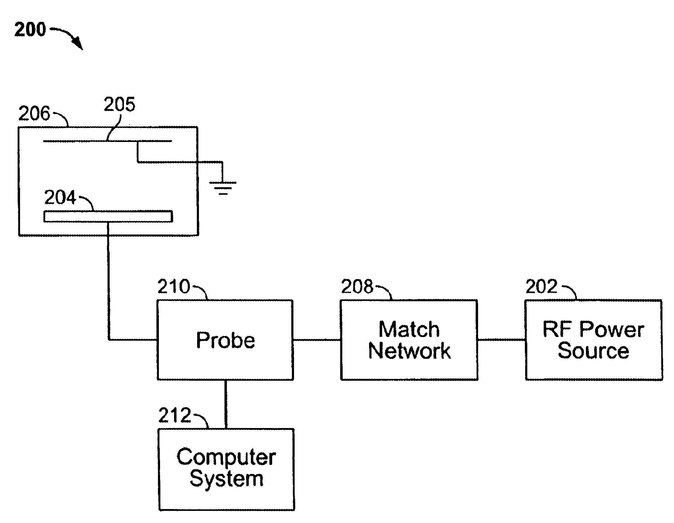
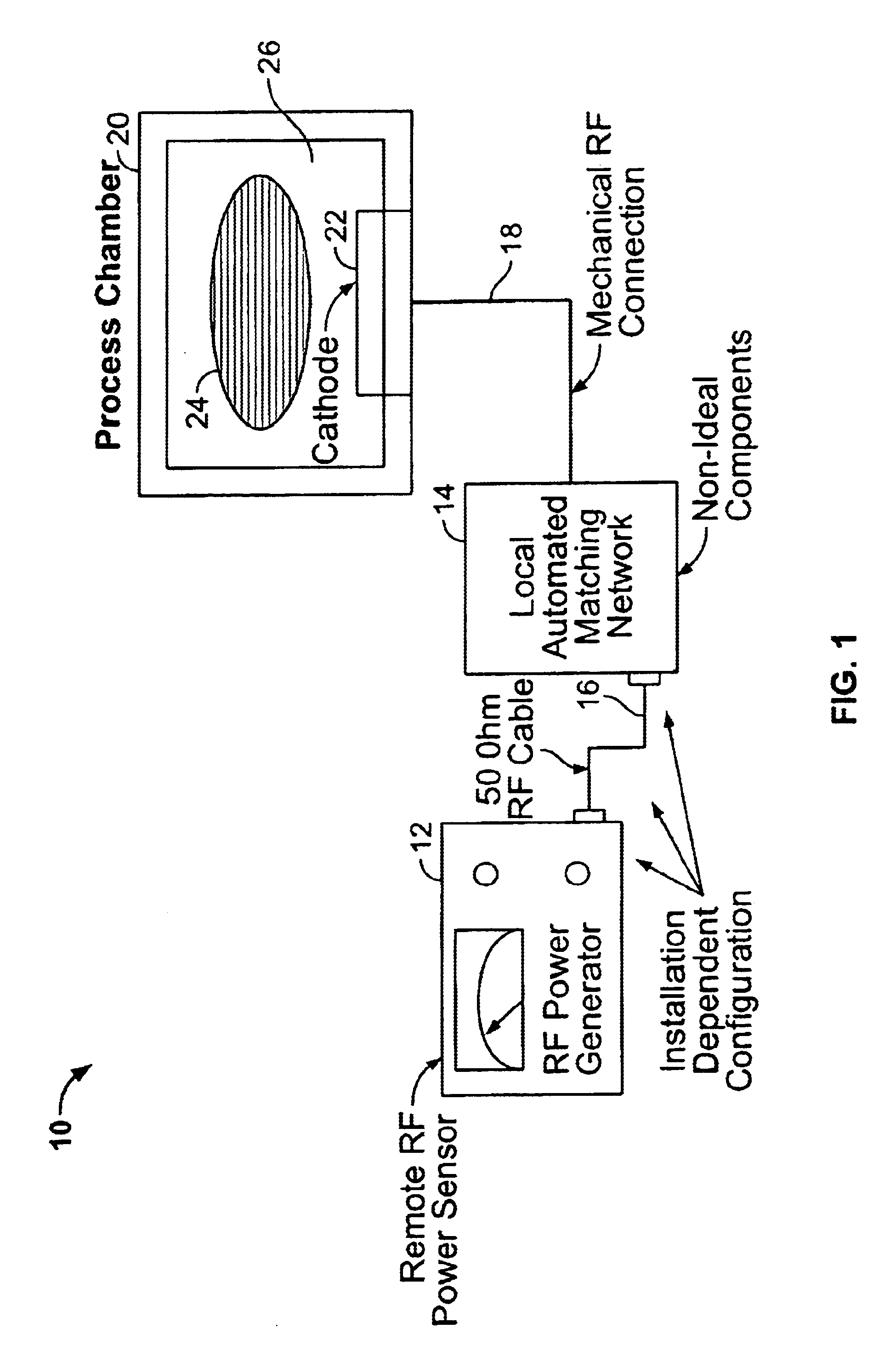
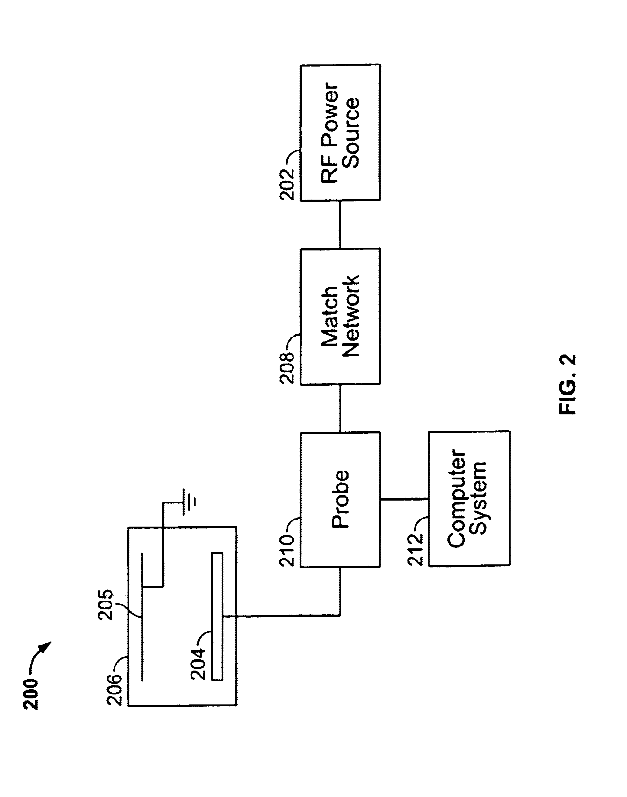
Embodiments of the present invention are described herein in the context of a plasma processing system. Those of ordinary skill in the art will realize that the following detailed description of the present invention is illustrative only and is not intended to be in any way limiting. Other embodiments of the present invention will readily suggest themselves to such skilled persons having the benefit of this disclosure. Reference will now be made in detail to implementations of the present invention as illustrated in the accompanying drawings. The same reference indicators will be used throughout the drawings and the following detailed description to refer to the same or like parts.

In the interest of clarity, not all of the routine features of the implementations described herein are shown and described. It will, of course, be appreciated that in the development of any such actual implementation, numerous implementation-specific decisions must be made in order to achieve the develope...


PUM

PropertyMeasurementUnit
Fractionaaaaaaaaaa
Poweraaaaaaaaaa
Electric potential / voltageaaaaaaaaaa

Abstract

A method tests a plasma processing system having a chamber, an RF power source, and a matching network. An RF power signal is generated from the RF power source to the chamber without igniting any plasma within the chamber. The voltage of the RF power signal, the current of the RF power signal, and the phase of the RF power signal, received by the chamber is measured while holding other parameters affecting the chamber constant. A value representative of an impedance of the chamber is computed based on the voltage, the current, and the phase. The value is then compared with a reference value to determine any defects in the plasma processing system. The reference value is representative of the impedance of a defect-free chamber.

Description

FIELD OF THE INVENTIONThe present invention relates to the fabrication of an electronic device. More particularly, the present invention relates to a method and system for verifying a plasma processing system.BACKGROUND OF THE INVENTIONVarious forms of processing with ionized gases, such as plasma etching and reactive ion etching, are increasing in importance particularly in the area of semiconductor device manufacturing. Of particular interest are the devices used in the etching process. Capacitively and inductively coupled plasma etching systems may be used in the processing and fabrication of semiconductor devices. A plasma processing system typically includes a plasma reactor having a plasma chamber therein. An RF power generator supplies RF power to the plasma chamber.As the principal driving force in plasma formation, the RF frequency and power should be the most carefully controlled parameter. Unfortunately, this is most typically not the case. FIG. 1, for example, shows RF n...

Claims


Application Information

Patent Timeline
IPC IPC(8): H01J37/32
CPCH01J37/32935H01J37/32082H01J37/304H01J37/3023
Inventor AVOYAN, ARMENJAFARIAN-TEHRANI, SEYED JAFAR
Owner LAM RES CORP
Why Eureka
Try Eureka