Display apparatus using luminance modulation elements
a technology of luminance modulation and display apparatus, which is applied in the direction of cathode-ray/electron beam tube circuit elements, static indicating devices, instruments, etc., can solve the problem that the capacitance of luminance modulation elements has become a factor of large power consumption, and achieve low power consumption, effective energy use, and low power consumption
- Summary
- Abstract
- Description
- Claims
- Application Information
AI Technical Summary
Benefits of technology
Problems solved by technology
Method used
Image

Examples
first embodiment
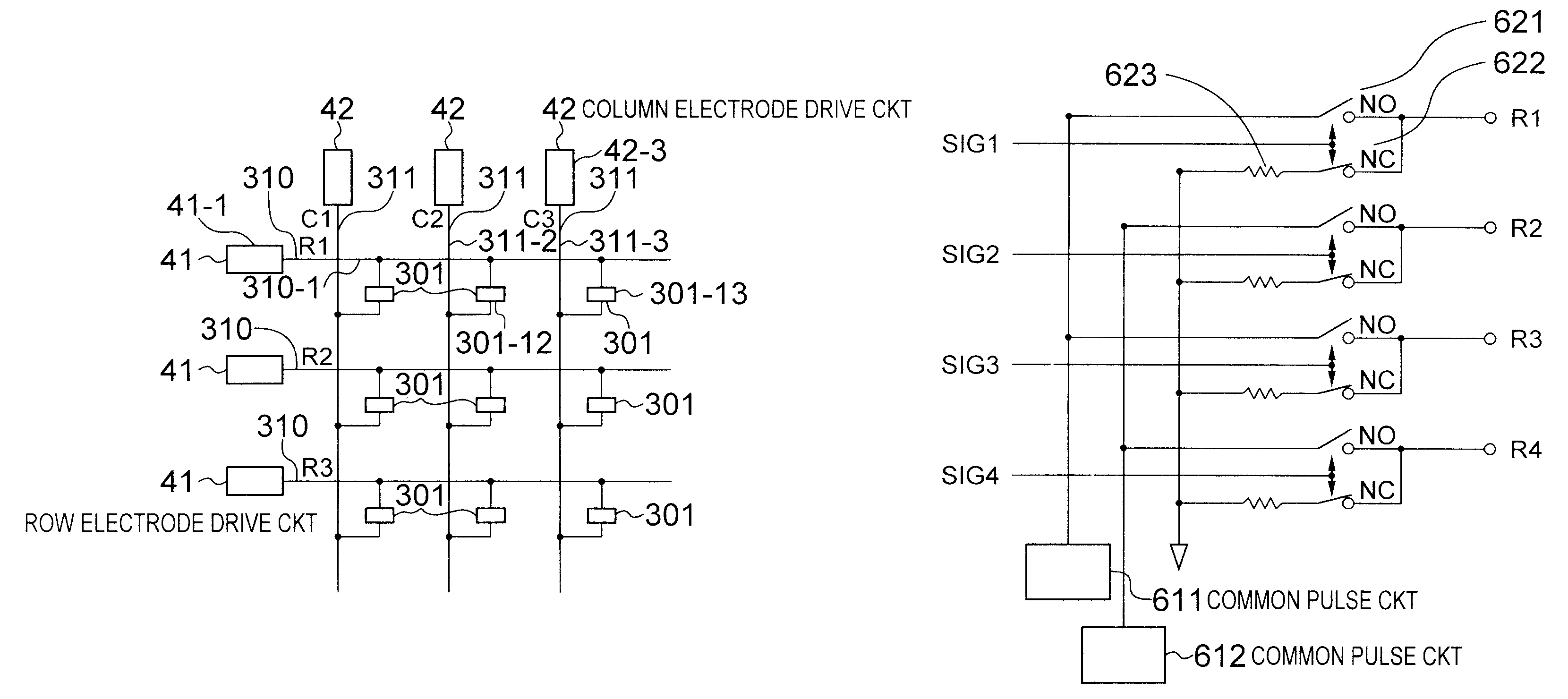
A display apparatus of a first embodiment according to the present invention is formed by using a display panel in which luminance modulation elements of dots are formed of a combination of a thin film electron emitter matrix serving as an electron emission source and a phosphor material, and by connecting drive circuits to row electrodes and column electrodes of the display panel.
The thin film electron emitter is an electron emission element having such a structure that an electron acceleration layer such as an insulation layer is inserted between two electrodes (a top electrode and a base electrode). The thin film electron emitter emits hot electrons accelerated in an electron acceleration layer into a vacuum through the top electrode. As examples of the thin film electron emitter, there are known an MIM electron emitter formed of metal, insulator and metal; a ballistic electron surface emission element using porous silicon or the like for the electron acceleration layer (describe...
second embodiment
A display panel used in a display apparatus of a second embodiment of the present invention, and a connection method between the display panel and drive circuits are the same as those of the first embodiment.
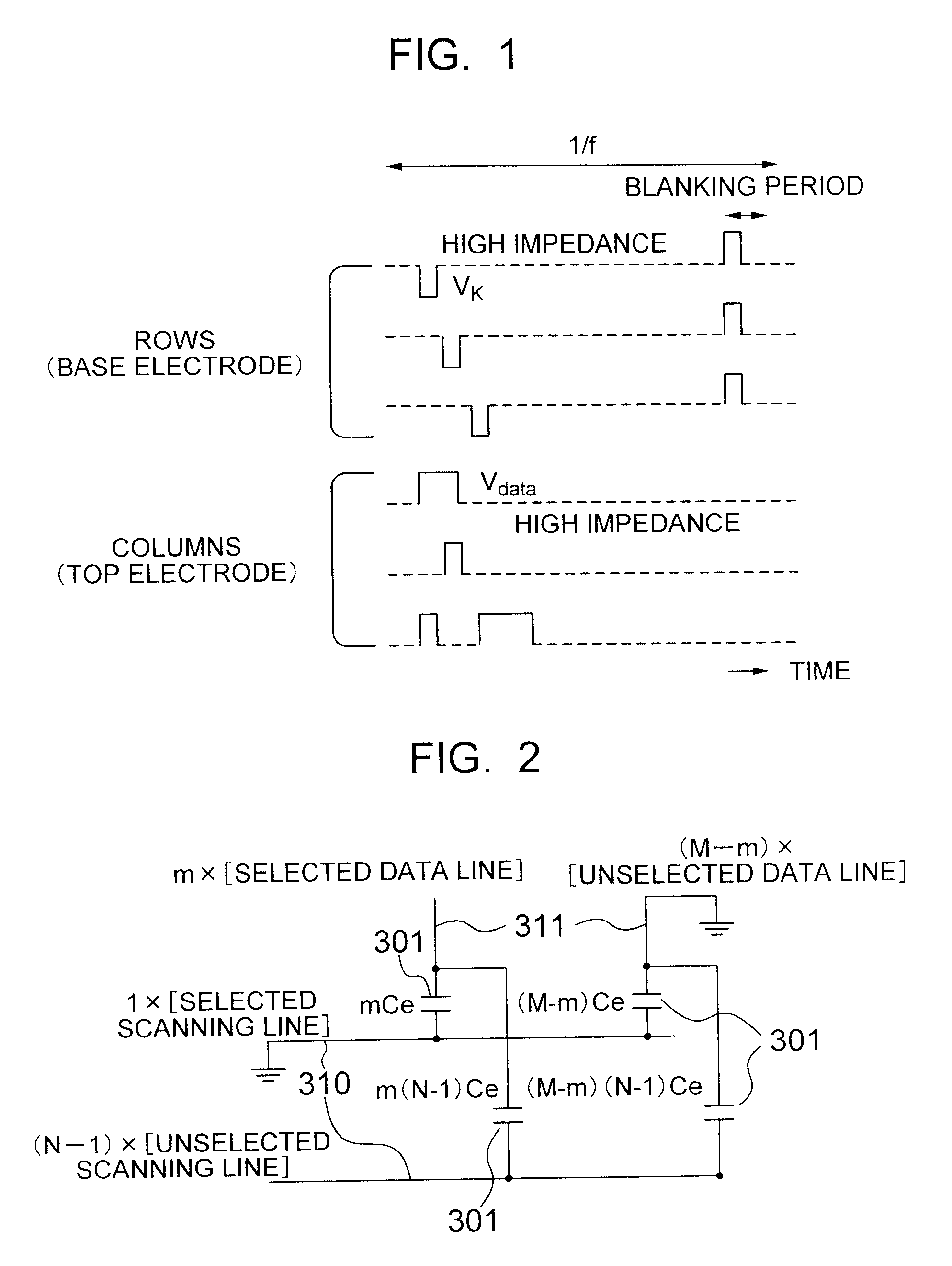
FIG. 18 is a timing chart showing an example of waveforms of drive voltages outputted from the row electrode drive circuits 41 and the column electrode drive circuits 42 in a display apparatus of a second embodiment of the present invention.
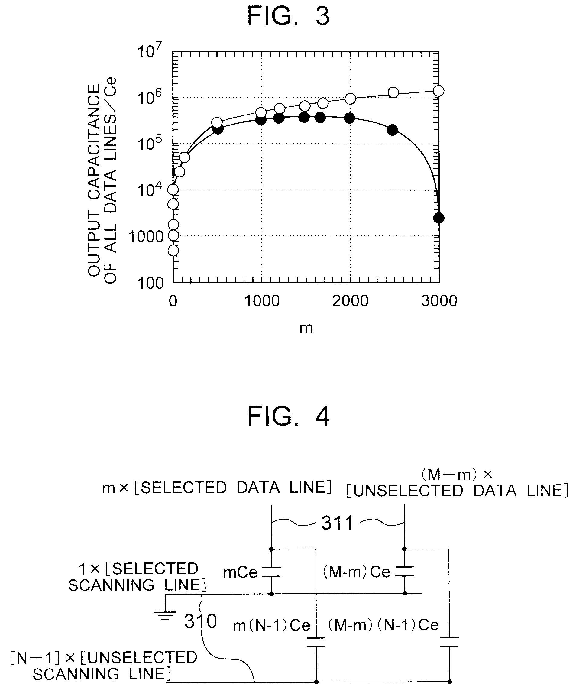
In an interval between time t1 and time t2, a scanning pulse having a potential of VR1 is applied to the row electrode (310) R1. Thereafter, in an interval between time t2 and time t3, a scanning pulse is applied to the row electrode (310) R2 to control electron emission of a thin film electron emitter located on the row electrode (310) R2. At this time, the adjacent row electrode (310) R1 is connected to the ground potential via a low impedance instead of the high impedance. Also when applying a scanning pulse to the row electrode (310) R3 i...
third embodiment
A configuration of a display panel used in an image display apparatus of a third embodiment according to the present invention will now be described by referring to FIG. 22.
A display panel used in the present embodiment is almost the same as that of the first embodiment. As shown in FIG. 22, however, the display panel used in the present embodiment differs from that of the first embodiment in that thin film electron emitter elements are formed as dummy pixels 303. The number of columns in which thin film electron emitter elements are formed as dummy pixels 303 is made larger than γ0M, where γ0 is a γ0 value represented by the expression (9). The dummy pixels 303 are formed between every row electrode 310 and each of the dummy column electrodes 313. Each of the dummy column electrodes 313 is connected to a dummy column electrode drive circuit 45.
However, phosphor materials 114 on a phosphor plate are formed in a region corresponding to a region surrounded by a broken line in FIG. 22....
PUM
 Abstract
Description
Claims
Application Information
 - R&D
- Intellectual Property
- Life Sciences
- Materials
- Tech Scout
- Unparalleled Data Quality
- Higher Quality Content
- 60% Fewer Hallucinations
Browse by: Latest US Patents, China's latest patents, Technical Efficacy Thesaurus, Application Domain, Technology Topic, Popular Technical Reports.
© 2025 PatSnap. All rights reserved.Legal|Privacy policy|Modern Slavery Act Transparency Statement|Sitemap|About US| Contact US: help@patsnap.com