Optical module and method of assembling the optical module

a technology of optical modules and optical modules, applied in the field of optical modules, can solve the problems of aconsiderable increase in the cost of optical modules, and achieve the effects of reducing the number of working steps required for assembling the optical modules, high accuracy, and high precision

Inactive Publication Date: 2005-04-05
JAPAN AVIATION ELECTRONICS IND LTD
View PDF17 Cites 17 Cited by
  • Summary
  • Abstract
  • Description
  • Claims
  • Application Information

AI Technical Summary

Benefits of technology

It is an object of the present invention to provide an optical module in which an assembling process of its optical coupling part can be simplified.
In accordance with the present invention, the alignment between the light receiving elements or the light emitting elements of the optical element and the end surfaces of the optical fibers of the optical fiber array is carried out by image recognition thereof. Accordingly, it is unnecessary to provide precise markers on the substrate at high accuracy as in the prior art as well as to mount the optical element on the substrate with high precision. As a result, the number of working steps required in assembling the optical module can be remarkably decreased, and the assembling work of the optical coupling part of the optical module can be simplified. Moreover, it is possible to reduce the manufacturing cost of the optical module.

Problems solved by technology

For that reason, in the prior art, a large number of working steps are needed in assembling the optical coupling part of the optical module, which results in a considerable increase of the cost of the optical module.

Method used


Image

  • Optical module and method of assembling the optical module
  • Optical module and method of assembling the optical module
  • Optical module and method of assembling the optical module

Examples


Embodiment Construction

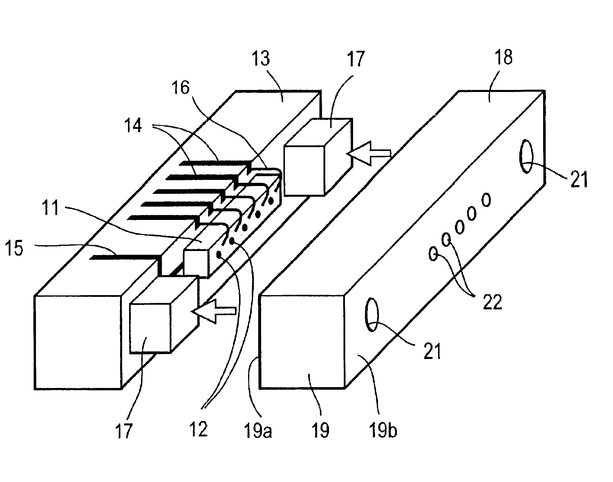
The preferred embodiment of the present invention will now be described in detail with reference to FIGS. 1 to 4. The present invention may, however, be embodied in many different forms and should not be construed as limited to the embodiment set forth hereinafter; rather, the embodiment is provided so that this disclosure will be thorough and complete, and will fully convey the scope of the invention to those skilled in the art.

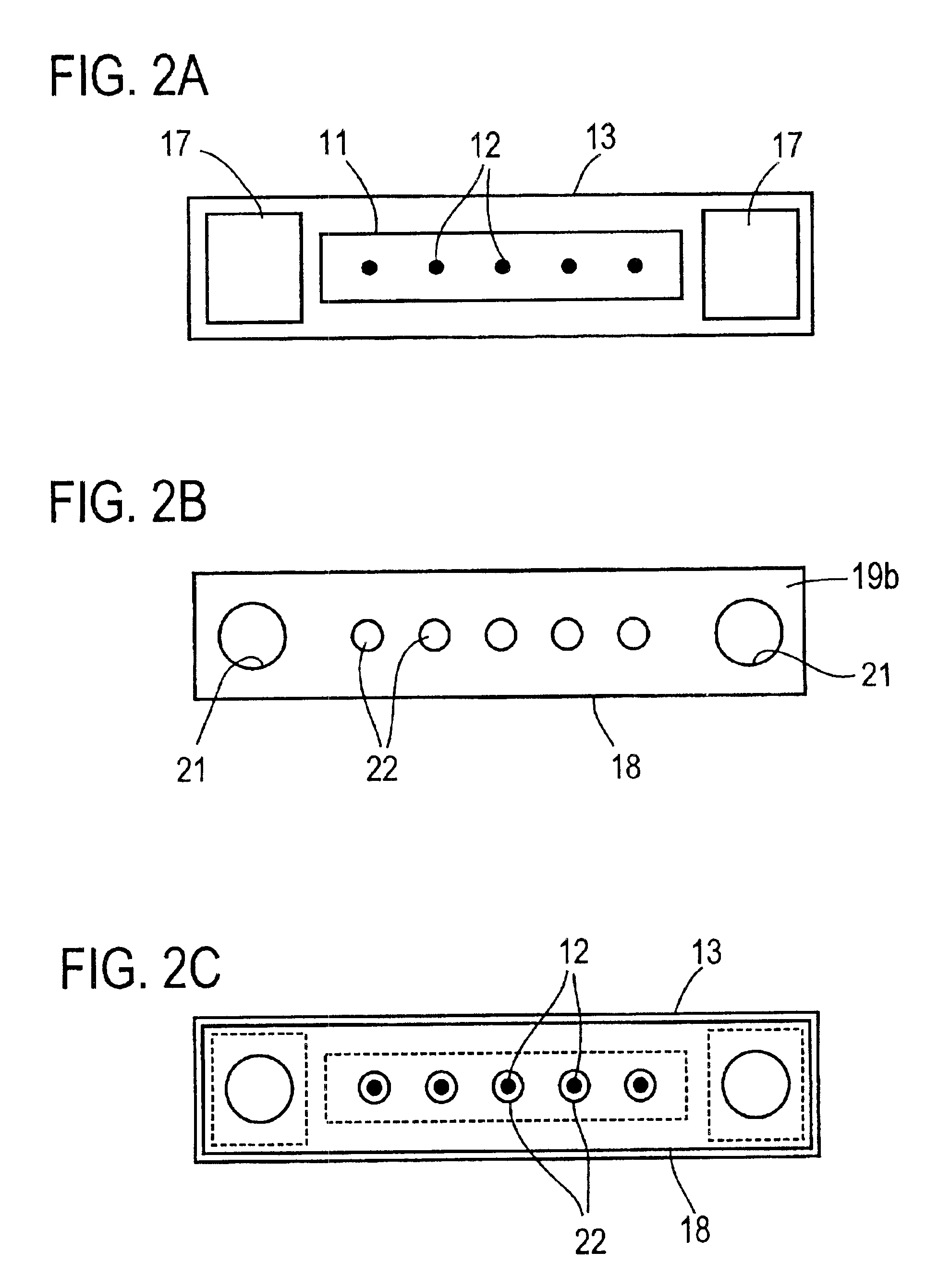
FIG. 1 is an exploded perspective view showing the construction of an embodiment of the optical module according to the present invention, FIG. 2 is diagrammatical views for explaining the manner that an alignment between light receiving elements of an optical device and optical fibers of an optical fiber array is carried out by image or picture recognition thereof, and FIG. 3 is diagrammatical views for explaining the mounting work of the optical fiber array. Further, this embodiment is a case that the present invention is applied to an optical module that ...


PUM


Abstract

There are provided an optical module in which an assembling process of its optical coupling part can be simplified, and a method of assembling the optical module. After a surface light receiving type or a surface light emitting type optical element has been mounted on a substrate, in case of mounting an optical fiber array to the substrate with a spacer or spacers interposed between the substrate and the optical fiber array, the optical fiber array is mounted and fixed to the substrate with the spacer or spacers interposed therebetween while alignment between a plurality of light receiving elements or light emitting elements of the optical element and the end surfaces of a plurality of optical fibers of the optical fiber array is being carried out by image recognition thereof.

Description

BACKGROUND OF THE INVENTION1. Field of the InventionThe present invention relates to an optical module provided with a surface light emitting type optical element or surface light receiving type optical element, and a method of assembling the optical module.2. Description of the Related ArtAn optical module that is capable of transmitting a plurality of optical signals is provided with a surface light emitting type optical element (it is also called an optical device) such as, for example, an laser diode array, and transmits optical signals emitted from the surface light emitting type optical element to an external circuit, device, apparatus or the like through an optical transmission path or line such as, for example, an optical fiber array. Also, an optical module that is capable of receiving a plurality of optical signals is provided with a surface light receiving type optical element (it is also called an optical device) such as, for example, a photodiode array, and receives opt...

Claims


Application Information

Patent Timeline
Patent Type & Authority Patents(United States)
IPC IPC(8): G02B6/42G02B6/38H01L31/0232H01S5/022
CPCG02B6/421G02B6/4249G02B6/4221G02B6/4292G02B6/42
Inventor NISHIMURA, TETSUYA
Owner JAPAN AVIATION ELECTRONICS IND LTD
Why Eureka
Try Eureka