Semiconductor device and its production method

a semiconductor and production method technology, applied in the direction of semiconductor devices, electrical appliances, transistors, etc., can solve the problems of increasing the diffusion distance of dopants, increasing the crystal defect, and increasing the leakage current, so as to simplify the manufacturing method of semiconductor devices, easy removal with ashing process

Inactive Publication Date: 2005-04-05
SHARP KK
View PDF11 Cites 14 Cited by
  • Summary
  • Abstract
  • Description
  • Claims
  • Application Information

AI Technical Summary

Benefits of technology

According to this embodiment, the first film, which needs to function as a mask two times, is formed of a layer-stacked film resistant to ashing process or hydrofluorination process, while the second f

Problems solved by technology

Forming a well having such a very large depth would indispensably involve injection of very high energy, leading to an increase in crystal defect as a result.
This in turn would incur an increase in leak current due to the crystal defects.
Further, high-temperature anneali

Method used


Image

  • Semiconductor device and its production method
  • Semiconductor device and its production method
  • Semiconductor device and its production method

Examples


embodiment 1

Embodiment 1 of the present invention is described with reference to FIGS. 1, 2, 3A, 3B, 3C, 3D, 3E, 3F and 4.

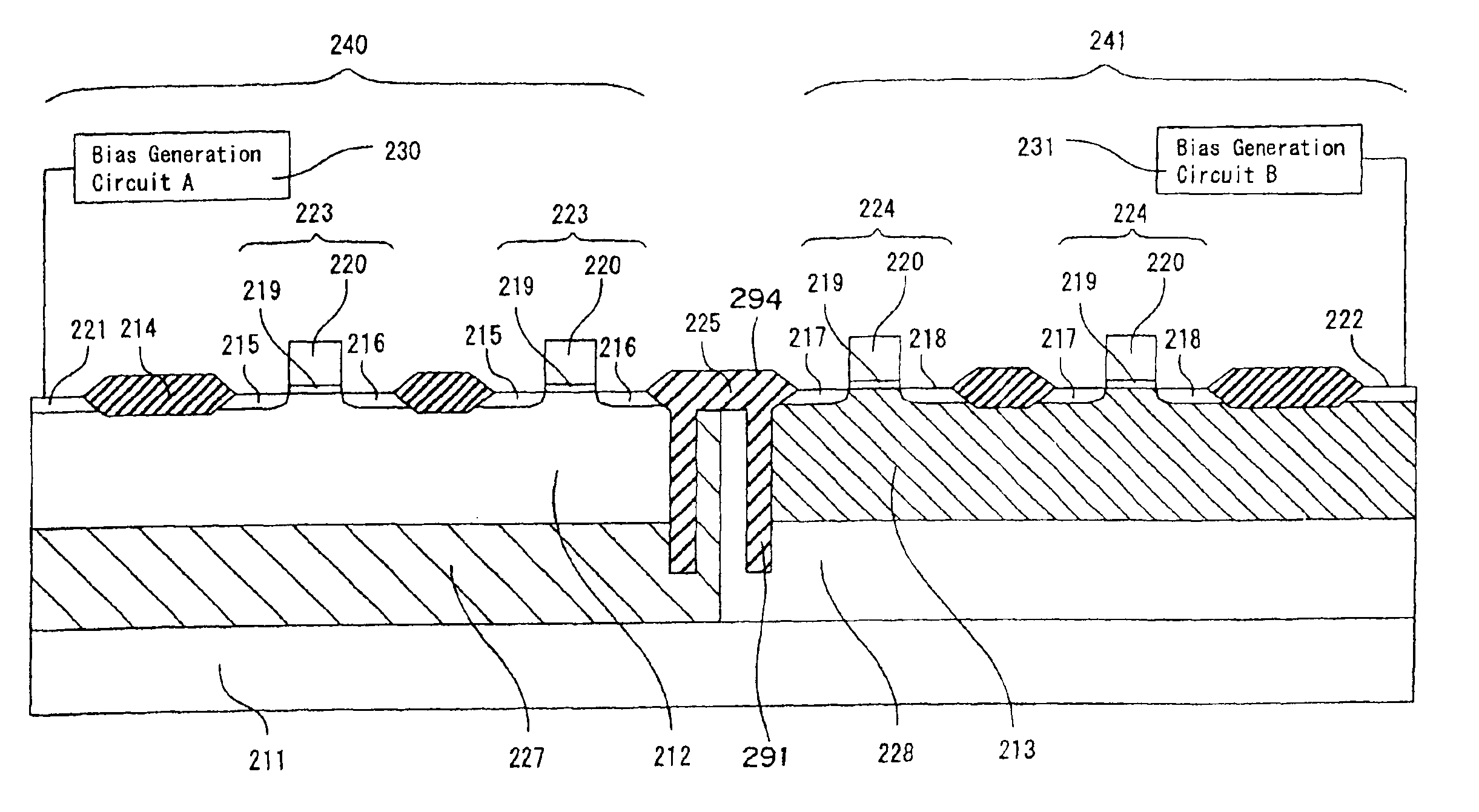
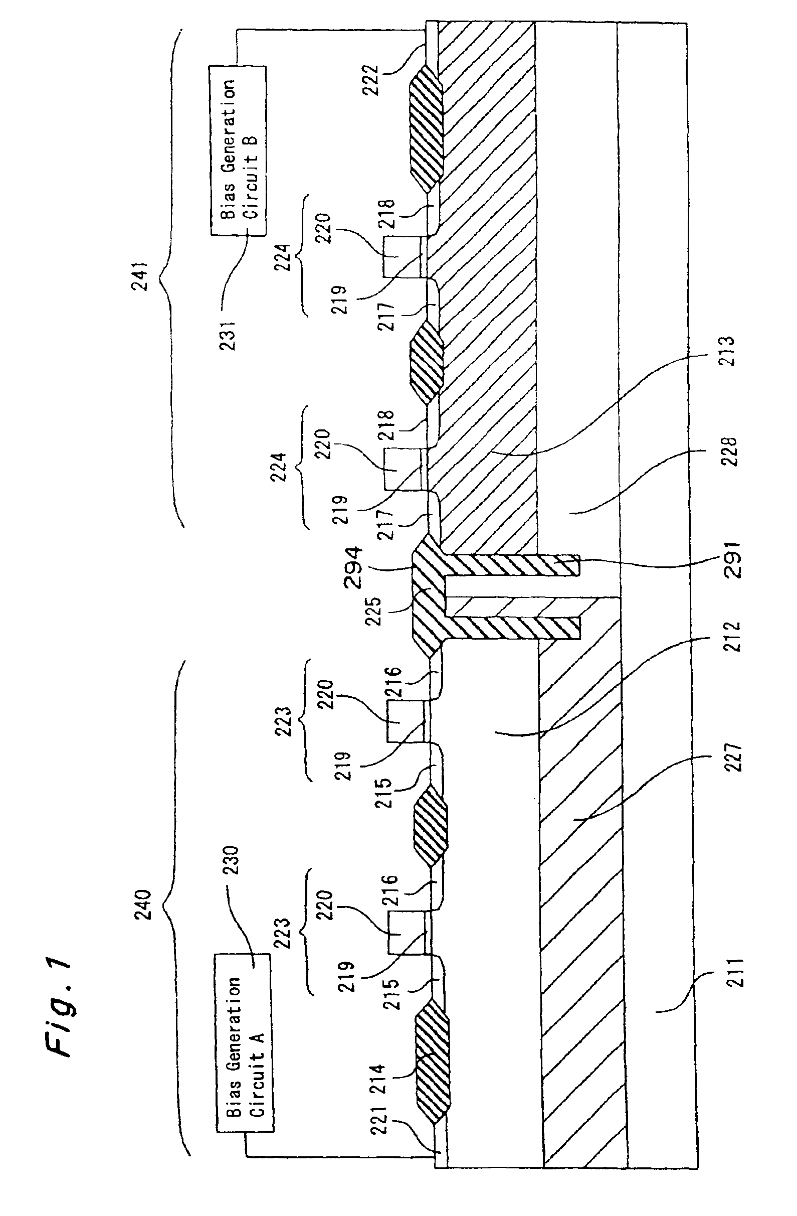
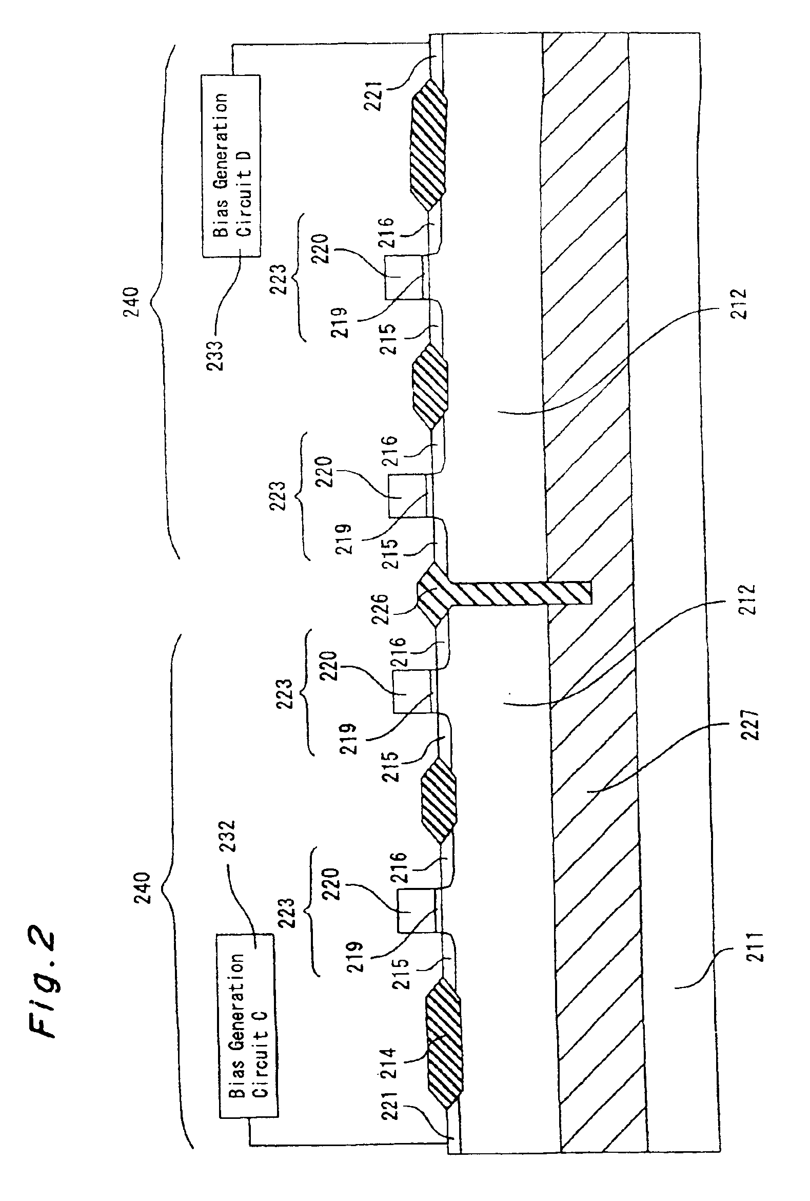
FIGS. 1 and 2 are schematic view each showing a cross section of a semiconductor device according to Embodiment 1 of the present invention. FIG. 1 shows a basic circuit block 240 composed of N-type substrate-bias variable transistors 223, 223, . . . , a basic circuit block 241 composed of P-type substrate-bias variable transistors 224, 224, . . . , and boundaries of these blocks. FIG. 2 shows two basic circuit blocks 240, 240 each composed of N-type substrate-bias variable transistors 223, 223, . . . , and a boundary of these blocks.

In the semiconductor device of this Embodiment 1, as shown in FIG. 1, an N-type deep well region 227 and a P-type deep well region 228 are formed in a semiconductor substrate 211.

A P-type shallow well region 212 is formed in the N-type deep well region 227. An N-type source region 215 and an N-type drain region 216 are formed in the P-type shallo...

embodiment 2

Embodiment 2 of the present invention is described with reference to FIGS. 5, 6A, 6B, 6C, 6D, 6E, 6F, 7A, 7B, 8, 9A, 9B, 9C, 9D and 9E.

FIG. 5 is a schematic view of a cross section of a semiconductor device which is Embodiment 2 of the present invention, showing a basic circuit block 240 composed of N-type substrate-bias variable transistors 223, a basic circuit block 241 composed of P-type substrate-bias variable transistors 224 and a boundary of these blocks.

The semiconductor device of this Embodiment 2 differs from the semiconductor device of the foregoing Embodiment 1 in the structure of the device isolation region. More specifically, the device isolation region of this Embodiment 2 is composed of two types of device isolation regions different in depth from each other, the shallower device isolation region being formed of STI (Shallow Trench Isolation).

Substrate-bias variable transistors 223 or 224 present within one basic circuit block 240 or 241 are isolated from each other b...

embodiment 3

Embodiment 3 of the present invention is explained with reference to FIG. 10 as follows.

FIG. 10 is a schematic view of a cross section of a semiconductor device which is Embodiment 3 of the invention, showing a basic circuit block composed of N-type substrate-bias variable transistors 326, a basic circuit block composed of P-type substrate-bias variable transistors 325, an N-type DTMOS 327, a P-type DTMOS 328 and boundaries of these.

In the semiconductor device of this Embodiment 3, an N-type deep well region 312 and a P-type deep well region 313 are formed in the semiconductor substrate 311.

A P-type shallow well region 315 is formed in an N-type deep well region 312. An N-type source region 317 and an N-type drain region 318 are formed on the P-type shallow well region 315. Also, a gate electrode 324 is formed via a gate insulator 323 on a channel region between the N-type source region 317 and the N-type drain region 318, by which an N-type substrate-bias variable transistors 326 a...


PUM


Abstract

A semiconductor device having a two-layer well structure and a small margin required at the boundary of a well region and comprising a substrate-bias variable transistor and a DTMOS. Field effect transistors (223) are formed on a P-type shallow well region (212). The depth of a shallow device isolation region (214) on the P-type shallow well region (212) is less than the depth of the junction between an N-type deep well region (227) and the P-type shallow well region (212). Therefore the field effect transistors (223) share the P-type shallow well region (212). The P-type shallow well regions (212) independently of each other are easily formed since they are isolated from each other by a deep device isolation region (226) and the N-type deep well region (227).

Description

TECHNICAL FIELDThe present invention relates to a semiconductor device including field effect transistors, such as MOSFETs (Metal Oxide Semiconductor Field Effect Transistors), and device isolation regions. More particularly, the invention relates to a semiconductor device in which voltage of well regions of the field effect transistors changes.BACKGROUND ARTAs a conventional method which is low in drive voltage to suppress off-leaks and still aimed at obtaining high drive current in CMOS (Complementary Metal Oxide Semiconductor) circuits using MOSFETs, there has been a method in which the well bias voltage is changed between standby and active states (see Japanese Patent Laid-Open Publications HEI 6-216346 and 10-340998).FIG. 16 shows a schematic cross-sectional view of a MOSFET in which the well bias is changed (hereinafter, the transistor will be referred to as substrate-bias variable transistor). Referring to FIG. 16, there are shown, with reference numerals having the following...

Claims


Application Information

Patent Timeline
IPC IPC(8): H01L21/762H01L21/70H01L21/761H01L21/8234H01L21/76H01L21/8238H01L27/08H01L27/092
CPCH01L21/761H01L21/76202H01L21/823493H01L21/823481H01L21/76232H01L27/06
Inventor IWATA, HIROSHISHIBATA, AKIHIDEKAKIMOTO, SEIZO
Owner SHARP KK
Why Eureka
Try Eureka