Organic light active devices and methods for fabricating the same

a technology of organic light and active devices, applied in the direction of final product manufacturing, sustainable manufacturing/processing, radiation control devices, etc., can solve the problems of light emission, and achieve the effects of simple manufacturing steps, long service life and long shelf li

Inactive Publication Date: 2005-04-05
DANIELS JOHN JAMES
View PDF17 Cites 129 Cited by
  • Summary
  • Abstract
  • Description
  • Claims
  • Application Information

AI Technical Summary

Benefits of technology

It is an object of the present invention to overcome the drawbacks of the prior art. In accordance with the present invention, a method is provided for fabricating OLED devices using field-attractive microcapsules. It is another object of the present invention to provide an OLED device that has a long shelf life, a long service life, is robust, effective and energy efficient. It is another object of the present invention to provide a method for fabricating an OLED device using relatively simple manufacturing steps and relatively uncomplicated fabrication equipment.
The OLED particulate may comprise organic-layered particles, each particle includes a hole transport layer and an electron emitter layer. A heterojunction is formed at the interface between the hole transport layer and the electron emitter layer. Each organic-layered particle may also include a blocking layer adjacent to the electron emitter layer and an emissive layer adjacent to the hole transport layer, thereby forming a stacked organic layered structure. The blocking layer is provided for facilitating the flow of electrons from the electron emitter layer, and the emissive layer is provided for facilitating the emission of photons when the energy state of the OLED particulate is raised.
As is described further here in, the microcapsule composition may be effective for enabling a “self healing” capability of the fabricated OLED device. In this case, the microcapsule includes a composition that causes the microcapsule to rupture if electrical energy above a threshold is applied to the microcapsule. For example, if a particular microcapsule is aligned so the during use of the OLED device it becomes a short between the electrodes, or if the microcapsule is adjacent to a dust particle or other foreign inclusion, creating such a short, when a electric potential is applied between the electrodes energy exceeding a predetermined threshold will pass through the microcapsule causing the capsule to rupture and disconnect the short. By this construction, the microcapsule is automatically removed from the path of conduction of electrical energy in the event of a short.
The typical OLED includes an OLED component that is a hole transport material and an OLED component that is an electron transport material. In accordance with a formulation of the inventive microcapsules, the shell comprises an OLED component material that is either the hole transport material or the electron transport material, and the internal phase of the microcapsule includes the OLED component material that is the other of the hole transport material and the electron transport material. Depending on the desired optical qualities of the fabricated OLED device, the carrier material can be selected so that it has optical properties during use of the OLED device that are transparent, diffusive, absorptive, and / or reflective to light energy. The composition of the OLED particulate can be selected so that the electrical characteristics of the OLED particulate includes, an electro or magneto rheological characteristic. This rheological characteristic is effective for causing the OLED particulate to move within the carrier and orient in response to an applied electrical or magnetic field.
To achieve a full color OLED display, the OLED particulate of the first OLED pixel layer emits light of a first wavelength range in response to a drive voltage being applied to the first layer electrode and the second layer electrode. Each subsequent OLED pixel layer emits light of a different wavelength range in response to the driving voltage applied to the respective electrode pairs so that an RGB color display can be formed.

Problems solved by technology

When an electric potential is applied to the electrodes, the electrical energy passes through the carrier material raising the energy state of the OLED particulate, resulting in the emission of light.

Method used


Image

  • Organic light active devices and methods for fabricating the same
  • Organic light active devices and methods for fabricating the same
  • Organic light active devices and methods for fabricating the same

Examples


Embodiment Construction

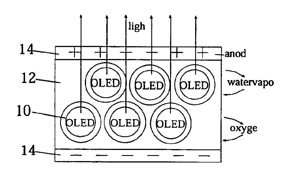
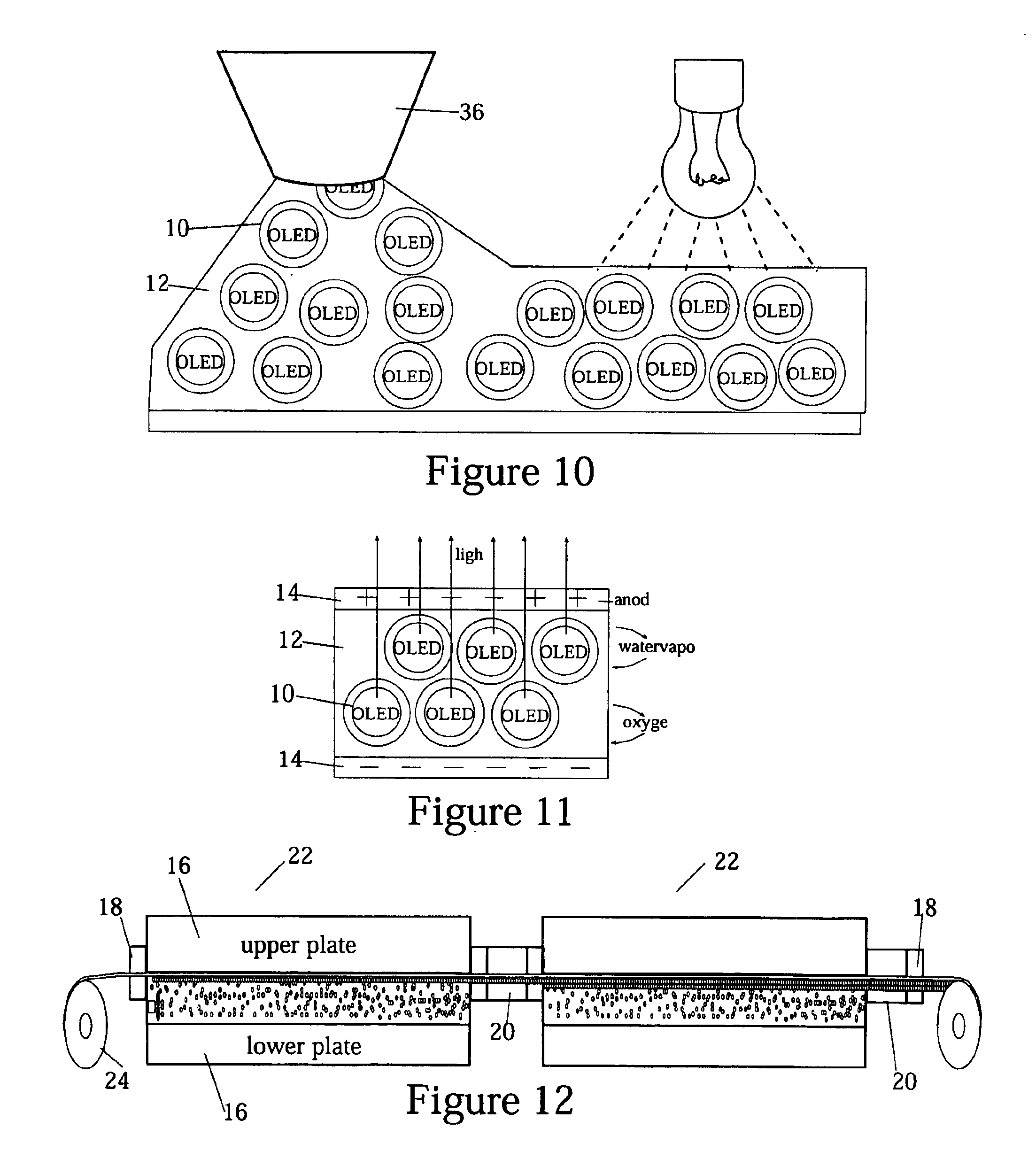
For purposes of promoting an understanding of the principles of the invention, reference will now be made to the embodiments illustrated in the drawings and specific language will be used to describe the same. It will nevertheless be understood that no limitation of the scope of the invention is thereby intended, there being contemplated such alterations and modifications of the illustrated device, and such further applications of the principles of the invention as disclosed herein, as would normally occur to one skilled in the art to which the invention pertains.

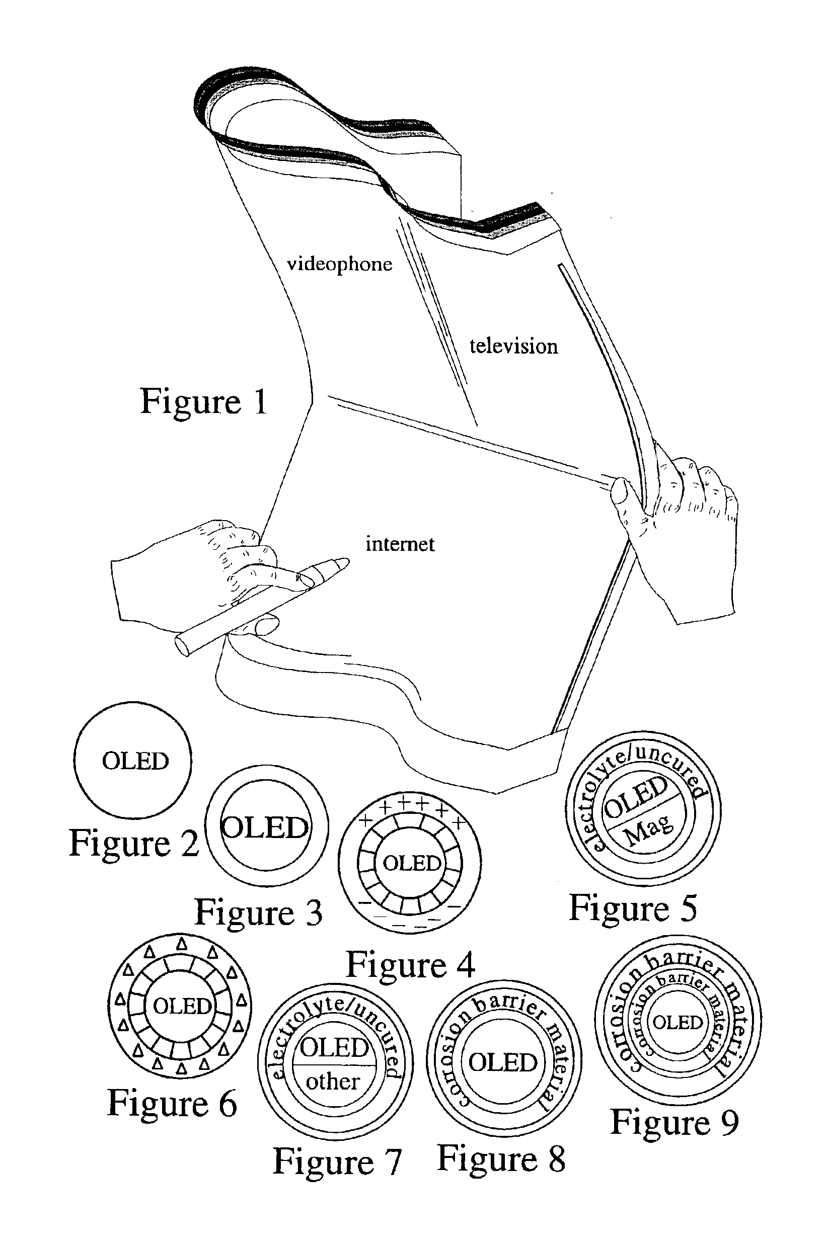
FIG. 1 illustrates an embodiment of the inventive thin, lightweight, flexible, bright wireless display having components capable of being manufactured by the inventive display fabrication method, showing the simultaneous display of mapped hyperlinked content, a videophone stream and a broadcast TV stream. FIG. 1 illustrates an embodiment of an inventive thin, lightweight, flexible, bright, wireless display showing the simul...


PUM

PropertyMeasurementUnit
thickaaaaaaaaaa
electrical energyaaaaaaaaaa
electrical characteristicsaaaaaaaaaa

Abstract

A method for fabricating organic light active devices using field-attractive Organic Light Active Material (“OLAM™”) microcapsules. The OLAM microcapsules are randomly dispersed within a monomer carrier fluid that is injected or otherwise disposed between two electrodes. The OLAM microcapsules may include additives that impart rheological properties, and other electrical, mechanical, optical and magnetic properties. The OLAM microcapsules form chains between the electrodes when an aligning field is applied. Holding the aligning field to keep the chains formed, the carrier fluid is cured and the OLAM microcapsule chains are locked into alignment between the electrodes. The problem of contamination of the OLAM material is the major factor limiting the display life span, and thus is a bar to commercial success. This fabrication method results in the corrosion sensitive OLAM material being protected by the microcapsule shell and the cured carrier, and the pixel alignment is automatic, since the OLAM microcapsule chains are formed only between the electrodes.

Description

BACKGROUND OF THE INVENTIONThe present invention pertains to organic light active devices. More particularly, the present invention pertains to devices and methods for fabricating organic light active devices that can be used for applications such as general lighting, display backlighting, video displays, maps, digital newspapers, stereoscopic vision aides, advanced vehicle windshields, solar cells, cameras and photodetectors.Organic light active material (“OLAM™”) makes use of the relatively recent discovery that polymers can be made to be conductors. Organic light emitting diodes (“OLED”) convert electrical energy into light, behaving as a forward biased pn junction. OLAMs can be light emitters or light detectors, depending on the material composition and the device structure. For the purpose of this disclosure, the term OLAM and OLED can be interchanged. In its basic form, an OLED is comprised of a layer of hole transport material upon which is formed a layer of electron transpor...

Claims


Application Information

Patent Timeline
Patent Type & Authority Patents(United States)
IPC IPC(8): H01L51/40H01L51/05H01L27/148H01L27/32H01L51/50
CPCH01L27/14627H01L27/148H01L27/3209H01L51/0004H01L51/5012H01L51/52H01L51/0003H01L27/3269Y02E10/549Y10S428/917H01J1/63Y02P70/50H10K59/32H10K59/13H10K71/13H10K71/12H10K50/11H10K50/80H10K50/182H01J63/04H05B33/00H01J1/62H10K50/00H10K59/00
Inventor DANIELS, JOHN JAMES
Owner DANIELS JOHN JAMES
Why Eureka
Try Eureka