Display device equipped with SRAM in pixel and driving method of the same

Inactive Publication Date: 2005-04-05
KK TOSHIBA
View PDF9 Cites 18 Cited by
  • Summary
  • Abstract
  • Description
  • Claims
  • Application Information

AI Technical Summary

Benefits of technology

An object of the present invention is to achieve a reduction in manufacturing costs by simpl

Problems solved by technology

Consequently, the difficulty of reducin

Method used


Image

  • Display device equipped with SRAM in pixel and driving method of the same
  • Display device equipped with SRAM in pixel and driving method of the same
  • Display device equipped with SRAM in pixel and driving method of the same

Examples


first embodiment

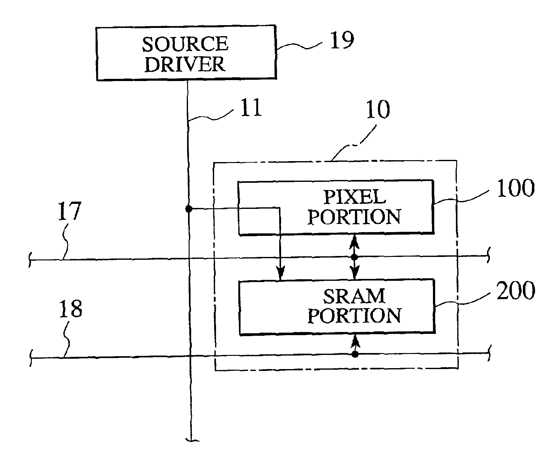
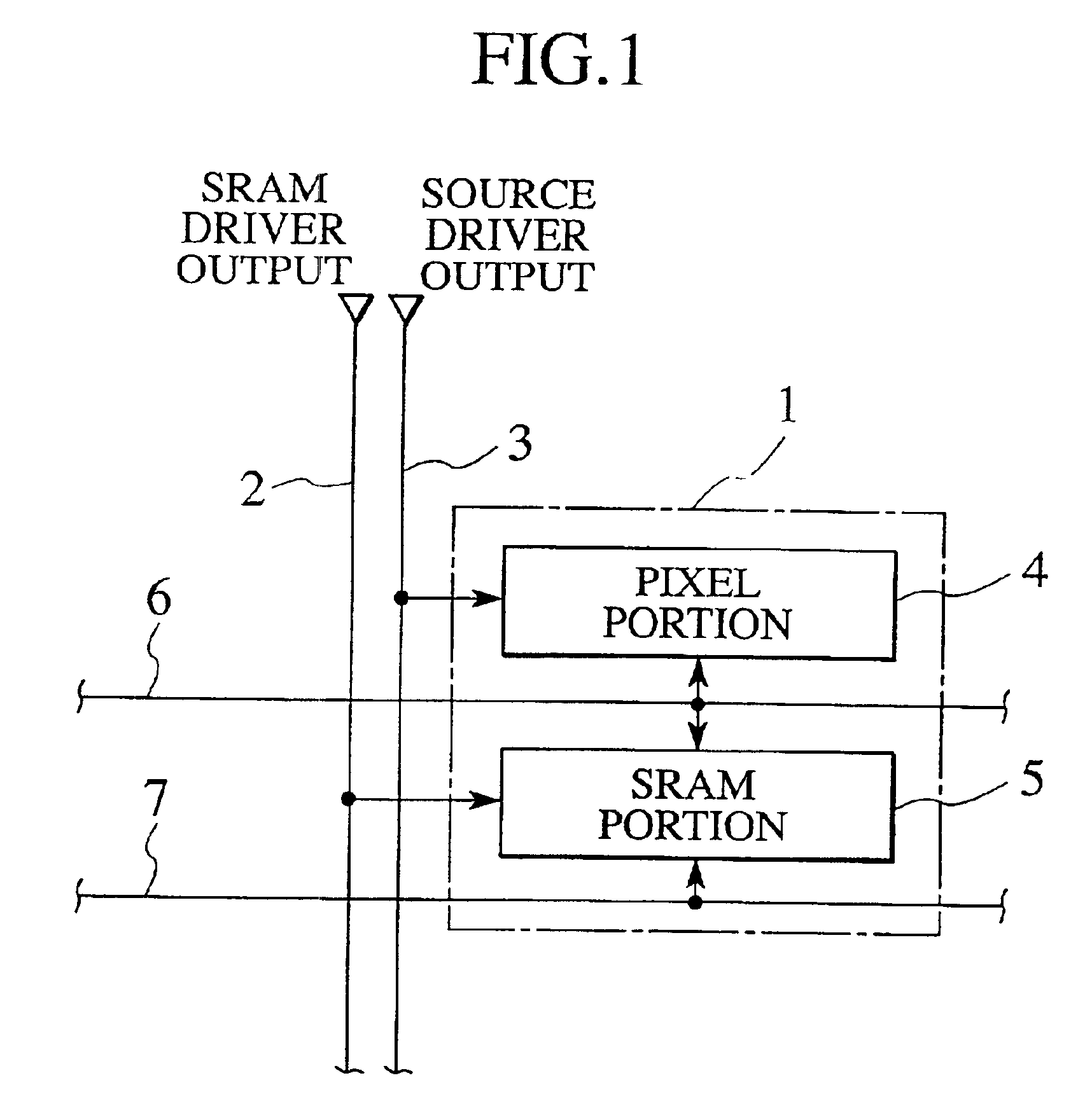
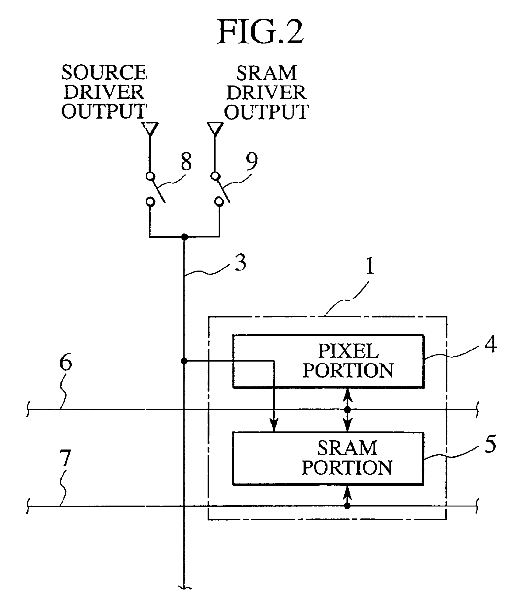
FIG. 3 shows a circuitry in one pixel of a liquid crystal display device according to the first embodiment. A pixel 10 shown in FIG. 3 includes a pixel portion 100 for executing display in accordance with a write voltage, and an SRAM portion 200 capable of holding binary data. Video data outputted from a source driver 19 is supplied through a signal line 11 to the pixel portion 100 and the SRAM portion 200. Reference numerals 17 and 18 denote a scanning line and an SRAM control line similar to those described above, respectively.

Though not shown in the drawing, pluralities of signal lines 11 and scanning lines 17 are present and disposed in a matrix form. The pixel 10 shown in FIG. 3 is disposed for each lattice of the matrix.

FIG. 4 shows the specific circuitry of the pixel portion 100 and the SRAM portion 200 shown in FIG. 3. A switch symbol in FIG. 4 represents a thin film transistor (TFT) switch such as MOSFET (n or p channel).

The pixel portion 100 includes a switch SW-P, a pixel...

second embodiment

FIG. 6 shows a circuitry in one pixel of a liquid crystal display device according to the second embodiment. In FIG. 6, portions similar to those of FIG. 4 are denoted by similar reference numerals. In FIG. 6, each of the switch symbols and the inverter symbols of FIG. 4 is represented by a circuit symbol indicating a TFT.

According to the second embodiment, a binary data conversion unit 300 is interposed between the pixel portion 100 and the SRAM portion 200. Accordingly, control lines X1, X2, 31, and 32 and a reference voltage line 21 are provided.

The binary data conversion unit 300 is designed to convert video data represented by a tone level of the normal display area into binary data corresponding to a brightest white display or a darkest black display in the pixel portion 100. The binary data conversion unit 300 includes a capacitor 22, an inverter 23, a loop switch 24, and a switch SW-V.

The capacitor 22 is a voltage holding circuit to hold a voltage in accordance with a potent...


PUM


Abstract

With regard to a display device having an SRAM incorporated in a pixel, a technology is disclosed, which is capable of reducing manufacturing costs by simplifying a constitution of a driver. A write voltage equivalent to white or black represented by a tone level of a normal display area is converted into a write voltage corresponding to a brightest white display or a darkest black display in the pixel, and is held in the SRAM of each pixel. In the case of normal display, display is carried out with the write voltage represented by the tone level of the normal display area. In the case of static image display, display is carried out with the write voltage corresponding to the brightest white display or the darkest black display in the pixel, the write voltage being held in the SRAM. Since the normal display and the static image display can be carried out with a write voltage supplied from one driver, the constitution of the driver can be simplified.

Description

CROSS-REFERENCE TO RELATED APPLICATIONSThis application is based upon and claims the benefit of priority under 35USC § 119 to Japanese Patent Application No. 2001-2631, filed Jan. 10, 2000; the entire contents of which are incorporated herein by reference.BACKGROUND OF THE INVENTION1. Field of the InventionThe present invention relates to a display device having an SRAM in a pixel. More specifically, the invention relates to a circuit technology for driving the SRAM.2. Description of the Related ArtA liquid crystal display device has been developed, which includes a memory element capable of holding video data statically. U.S. Pat. No. 5,712,652 discloses one of basic principles with regard to such a liquid crystal display device. The liquid crystal display device disclosed in U.S. Pat. No. 5,712,652 includes a memory cell in a pixel, and carries out static image display by using binary video data held in the memory cell, accordingly reducing power consumption in the static image di...

Claims


Application Information

Patent Timeline
IPC IPC(8): G09G3/36G09G3/20G02F1/133
CPCG09G3/3614G09G3/3648G09G2300/0857G09G2300/0842G09G2300/0809G09G3/36
Inventor MURATA, HIROYOSHIYAMASAKI, NOBUOKITANI, MASAKATSUAOKI, YOSHIHIRO
Owner KK TOSHIBA
Why Eureka
Try Eureka