Structure for preventing disconnection in liquid crystal display device and manufacturing method thereof

Active Publication Date: 2005-04-05
LG DISPLAY CO LTD
View PDF6 Cites 8 Cited by
  • Summary
  • Abstract
  • Description
  • Claims
  • Application Information

AI Technical Summary

Benefits of technology

An object of the present invention is to provide to a method for manufacturing an LCD devi

Problems solved by technology

Despite various technical developments in the LCD technology for applications in different fields, research for enhancing the picture quality of the LCD device has been in some respects lacking as compared to other features of the LCD device.
However, the polycrystalline silicon TFTs for the pixels have a high drain current value during the switch

Method used


Image

  • Structure for preventing disconnection in liquid crystal display device and manufacturing method thereof
  • Structure for preventing disconnection in liquid crystal display device and manufacturing method thereof
  • Structure for preventing disconnection in liquid crystal display device and manufacturing method thereof

Examples


Example

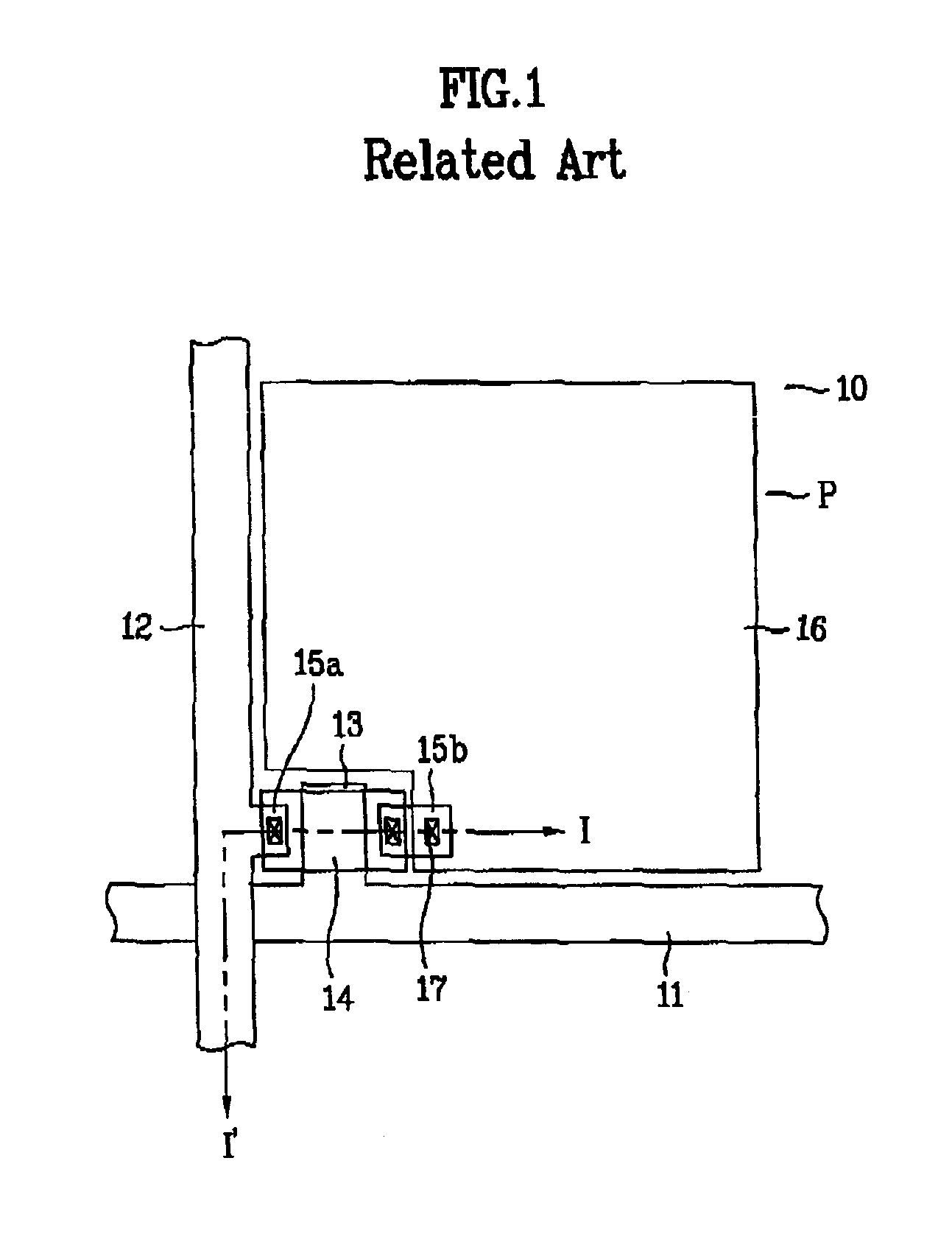
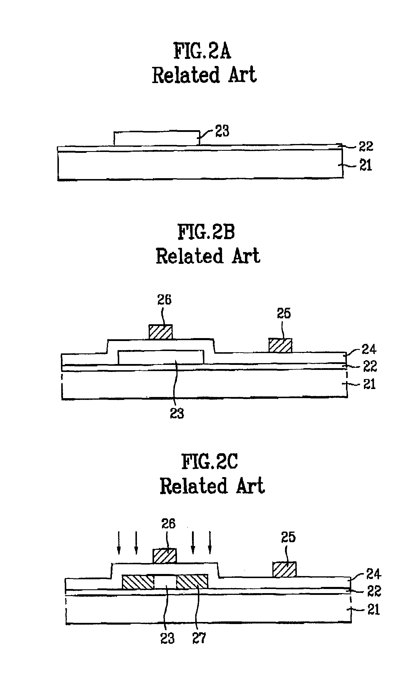
Reference will now be made in detail to the preferred embodiments of the present invention, examples of which are illustrated in the accompanying drawings. Wherever possible, the same reference numbers will be used throughout the drawings to refer to the same or like parts.

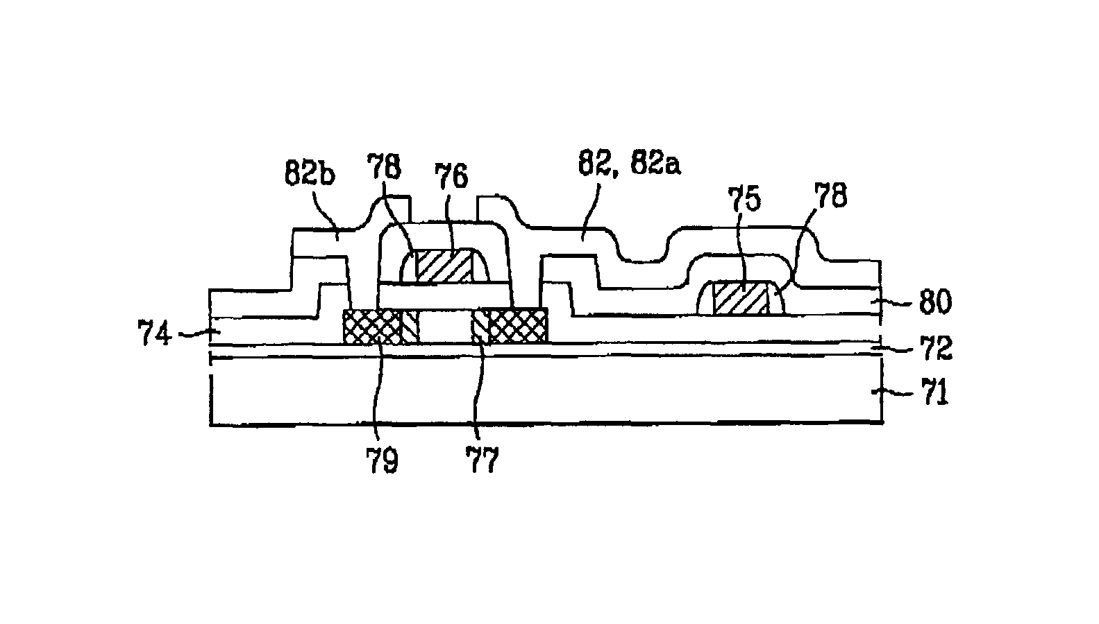
FIG. 5A to FIG. 5I are cross-sectional views illustrating manufacturing process steps of an LCD device according to an exemplary embodiment of the present invention. Referring to FIG. 5A, a buffer layer 52 of a silicon oxide material is formed on an insulating layer or TFT array substrate 51. An amorphous silicon layer is then formed on the buffer layer 52. The amorphous silicon is deposited on the buffer layer 42 at a temperature between about 300° C. and about 400° C. by Plasma Enhanced CVD (PECVD), Low-Pressure CVD (LPCVD) using silane gas by sputtering, or other like methods. Subsequently, a laser irradiates the amorphous silicon layer to crystallize the amorphous silicon layer to form a polycrystalline-silico...


PUM


Abstract

A method for manufacturing an LCD device having gate and data lines includes forming an active layer on an insulating substrate; forming a gate insulating layer over a surface of the insulating substrate including the active layer; forming a gate line and a gate electrode on the gate insulating layer, so that the gate electrode is positioned above the active layer; forming a photoresist pattern on the gate electrode and on the gate line where the gate and the data lines cross each other, wherein, the photoresist pattern surrounds the gate electrode and the gate line; forming source and drain regions in the active layer by injecting impurity ions into the active layer using the photoresist pattern as a mask; removing the photoresist pattern; forming an insulating interlayer over the entire surface of the insulating substrate, the insulating interlayer having first contact holes exposing predetermined portions of the source and drain regions; forming a data line electrically connected to the source region and crossing over the gate line on the insulating interlayer; forming a drain electrode; forming a passivation layer over the surface of the insulating substrate, the passivation layer having a second contact hole exposing a predetermined portion of the drain electrode; and forming a pixel electrode to electrically connect to the drain region through the second contact hole.

Description

This application claims the benefit of the Korean Application No. P2002-51184 filed on Aug. 28, 2002, which is hereby incorporated by reference in its entirety.BACKGROUND OF THE INVENTION1. Field of the InventionThe present invention relates to a method for manufacturing a liquid crystal display (LCD) device, and more particularly, to a structure and method for manufacturing an LCD device to prevent a disconnection of a data line.2. Discussion of the Related ArtAs the information society develops demands for various types of display devices increase. Accordingly, many efforts have been made to research and develop various flat display devices, such as liquid crystal displays (LCD), plasma display panels (PDP), electroluminescent displays (ELD), and vacuum fluorescent displays (VFD), and some species of the flat display devices are already applied to displays of various types of equipment. Among the species of flat display devices, the liquid crystal display (LCD) device has been mos...

Claims


Application Information

Patent Timeline
IPC IPC(8): G02F1/13G02F1/1362G02F1/133
CPCG02F1/136286G02F1/133
Inventor HWANG, KWANG JO
Owner LG DISPLAY CO LTD
Why Eureka
Try Eureka