Printing wiring board and method of producing the same and capacitor to be contained in printed wiring board

a technology of printed wiring board and printed circuit board, which is applied in the direction of printed circuit non-printed electric components association, sustainable manufacturing/processing, and final product manufacturing, etc., can solve the problems of small behavior of the capacitors incorporated in the core substrate, cracks and peelings that are not easily visible on the core substrate, etc., and achieve the effect of increasing reliability

Inactive Publication Date: 2005-04-05
IBIDEN CO LTD
View PDF17 Cites 155 Cited by
  • Summary
  • Abstract
  • Description
  • Claims
  • Application Information

AI Technical Summary

Benefits of technology

In accordance with aspects of the invention, a metal film is formed on the electrodes of the chip capacitors. As a result, the chip capacitor have a flat surface. When the chip capacitors are accommodated in the printed circuit board, and penetrating openings are formed in the resin which covers the electrodes, no resin is left. In this manner, the connection between the via holes and the electrodes has increased reliability.

Problems solved by technology

As a result, the behavior of the capacitors incorporated in the core substrate becomes small.
In this manner, even if internal stress is generated between the core substrate and the capacitors caused by the difference in the thermal expansion coefficients therebetween, cracks and peelings do not easily occur in the core substrate.

Method used


Image

  • Printing wiring board and method of producing the same and capacitor to be contained in printed wiring board
  • Printing wiring board and method of producing the same and capacitor to be contained in printed wiring board
  • Printing wiring board and method of producing the same and capacitor to be contained in printed wiring board

Examples


first embodiment

Hereinafter, embodiments of the present invention will be described with reference to the drawings.

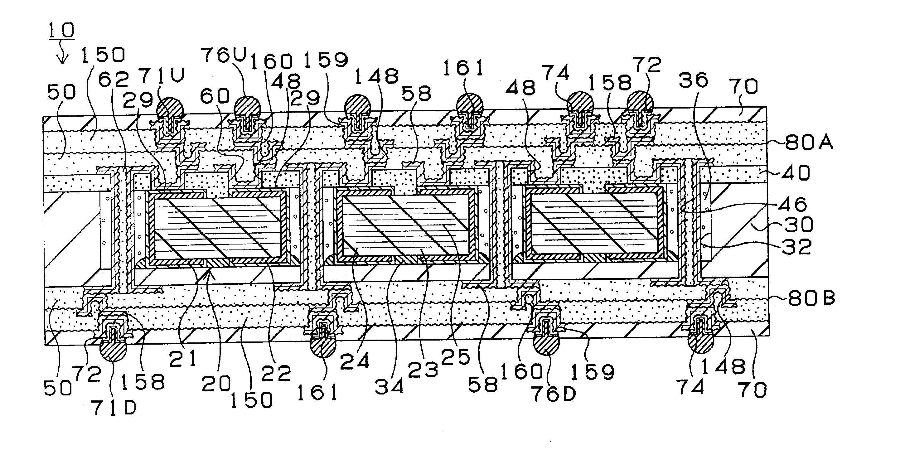
First, the structure of a printed circuit board according to a first embodiment of the present invention will be described with reference to FIGS. 7 and 8. FIG. 7 is a diagram showing across section of a printed circuit board 10. FIG. 8 is a diagram showing a state where an IC chip 90 is mounted on the printed circuit board 10 shown in FIG. 7, and the printed circuit board 10 is attached onto a daughter board 95.

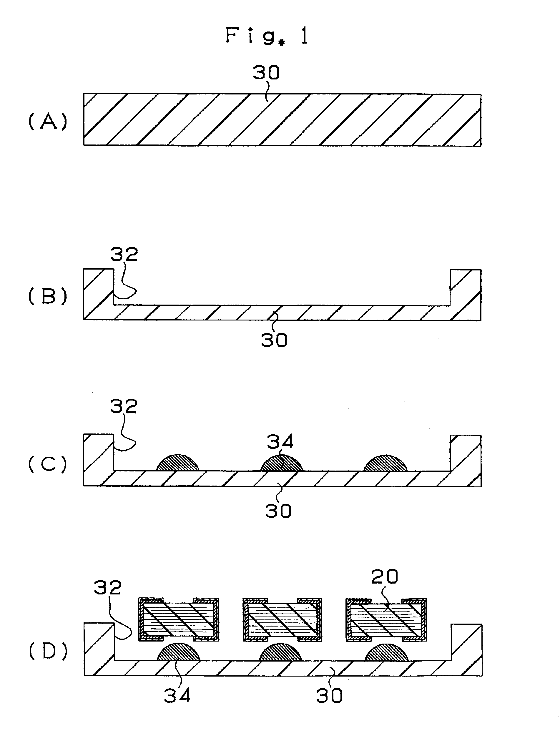
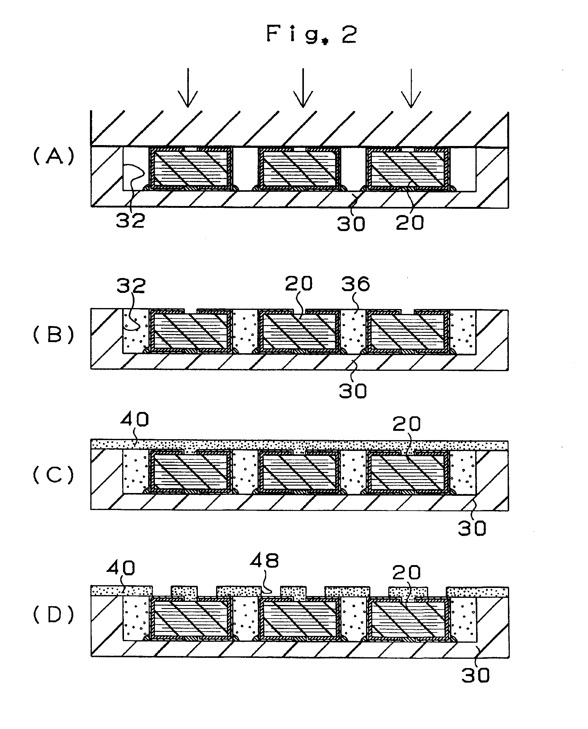
As shown in FIG. 7, the printed circuit board 10 is constituted by a core substrate 30 accommodating a plurality of chip capacitors 20, and a buildup circuit layers 80A, BOB. The buildup circuit layers 80A and 80B are constituted by an interlayer resin insulating layer 50 and 150. The interlayer resin insulating layer 50 has via holes 160 and conductor circuits 158. The interlayer resin insulating layer 150 has via holes 161 and conductor circuits 159. A solder resist layer 70 ...

second embodiment

First, the structure of a printed circuit board according to a second embodiment of the present invention will be described with reference to FIGS. 29 and 30. FIG. 29 is a diagram showing a cross section of a printed circuit board 210. FIG. 30 is a diagram showing the state where an IC chip 290 is mounted on the printed circuit board 210 shown in FIG. 29, and the printed circuit board 210 is attached to a daughter board 294.

As shown in FIG. 29, the printed circuit board 210 incorporates chip capacitors 220, a core substrate 230 for accommodating chip capacitors 220, and an interlayer resin insulating layer 250 constituting the buildup layers 280A, 280B. The core substrate 230 is constituted by an accommodating layer 230a for accommodating the capacitors 220, and a connection layer 240. Via holes 260 and a conductor circuit 258 are formed in the connection layer 240. Via holes 360 and a conductor circuit 358 are formed in the interlayer resin insulating layer 250. In this embodiment,...

third embodiment

First, the structure of a printed circuit board according to a third embodiment of the present invention will be described with reference to FIGS. 37 and 38. FIG. 37 is a diagram showing across section of a printed circuit board 410. FIG. 38 is a diagram showing the state where an IC chip 490 is mounted on the printed circuit board 410 shown in FIG. 37, and the printed circuit board 410 is attached to a daughter board 494.

As shown in FIG. 37, the printed circuit board 410 incorporates chip capacitors 420, a core substrate 430 for accommodating chip capacitors 420, and an interlayer resin insulating layer 450 constituting the buildup layers 480A, 480B. The core substrate 430 is constituted by an accommodating layer 430a for accommodating the capacitors 420, and a connection layer 440. Via holes 460 and a conductor circuit 458 are formed in the connection layer 440. Via holes 560 and a conductor circuit 558 are formed in the interlayer resin insulating layer 450. In this embodiment, t...


PUM

PropertyMeasurementUnit
temperatureaaaaaaaaaa
thicknessaaaaaaaaaa

Abstract

Chip capacitors 20 are provided in a printed circuit board 10. In this manner, the distance between an IC chip 90 and each chip capacitor 20 is shortened, and the loop inductance is reduced. In addition, the chip capacitors 20 are accommodated in a core substrate 30 having a large thickness. Therefore, the thickness of the printed circuit board does not become large.

Description

TECHNICAL FIELDThe present invention relates to a printed circuit board on which electric elements, such as IC chips, are mounted. More specifically, the present invention relates to a printed circuit board incorporating capacitors therein, and a method for manufacturing the same.BACKGROUND ARTIn a computer, the length of electric wiring between the power supply and the IC chip is usually long, and therefore, the loop inductance at this electric wiring is extremely large. The variation in the voltage at which the IC is driven in high-speed operation mode becomes very large accordingly, possibly causing malfunction of the IC. In addition, it becomes difficult to stabilize the voltage of the power supply. In an attempt to avoid these troubles, a capacitor is mounted on the surface of the printed circuit board as an auxiliary device for assisting the power supply operation.Specifically, the loop inductance which causes the variation in voltage depends on the length of electric wire fro...

Claims


Application Information

Patent Timeline
Patent Type & Authority Patents(United States)
IPC IPC(8): H01L23/50H01L23/64H01L21/02H01L23/498H01L23/58H01L23/48H01L21/48H01L25/16H05K1/18H05K3/46H05K1/02
CPCH01G4/224H05K1/183H01G4/40H01L21/4857H01L23/49822H01L23/49827H01L23/50H01L23/642H01L23/645H01L25/16H01L25/162H05K1/0231H05K1/185H05K1/186H01G4/228H01L23/498H01L2224/16225H01L2224/16227H01L2224/16237H01L2924/01002H01L2924/01005H01L2924/01011H01L2924/01012H01L2924/01015H01L2924/01018H01L2924/0102H01L2924/01025H01L2924/01027H01L2924/01046H01L2924/01051H01L2924/01074H01L2924/01078H01L2924/01079H01L2924/14H01L2924/15174H01L2924/15192H01L2924/15311H01L2924/15312H01L2924/19041H01L2924/19105H01L2924/19106H01L2924/30107H01L2924/3011H05K1/112H05K1/181H05K3/4602H05K2201/09509H05K2201/10636H05K2201/10674H01L2924/01019H01L2224/05573H01L2224/05568H01L2924/3511Y02P70/50H05K3/18H01L2224/05001H01L2224/05027H01L2224/05572H01L2224/05008H01L2224/05024H01G2/06H01G4/12H01G4/248H05K1/115H05K2201/09545H05K2201/096H05K2201/10015
Inventor INAGAKI, YASUSHIASAI, MOTOOWANG, DONGDONGYABASHI, HIDEOSHIRAI, SEIJI
Owner IBIDEN CO LTD
Why Eureka
Try Eureka