

Glitchless pulse generator
a glitchless, pulse technology, applied in the direction of pulse technique, generating/distributing signals, counting chain synchronous pulse counters, etc., can solve the problems of obviating the need for expensive all-purpose testing equipment for performing delay testing on chips, reducing errors at the expense of additional logic that occupies etc., to achieve the effect of reducing errors, reducing errors, and occupying more space on the chip
- Summary
- Abstract
- Description
- Claims
- Application Information
AI Technical Summary
Benefits of technology
Problems solved by technology
Method used
Image

Examples
Embodiment Construction
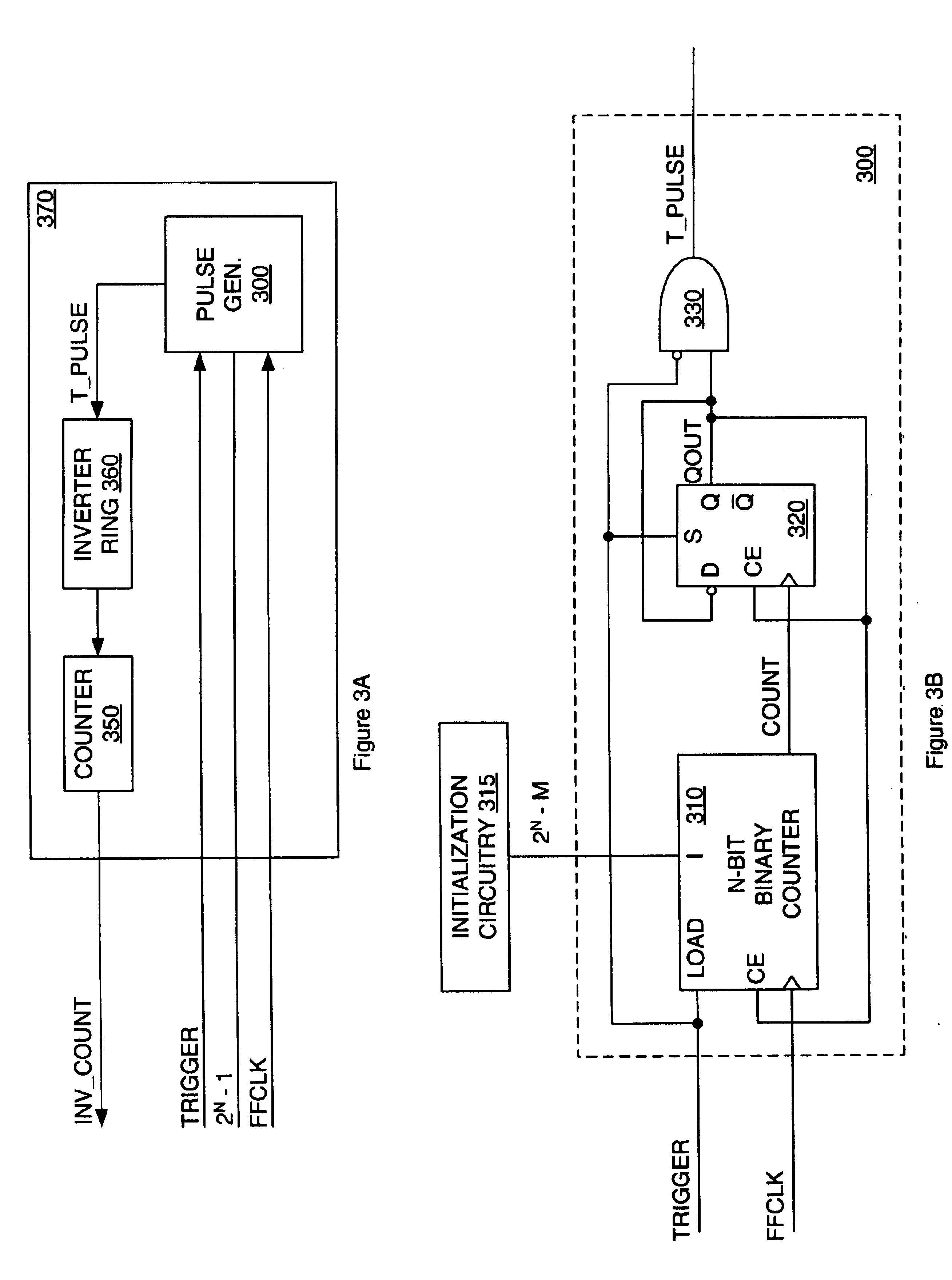
A pulse having a duration of T seconds may be generated using a clock signal having a frequency of X MHz. In one embodiment, this clock signal is generated by a crystal oscillator. A number of clock cycles M of the clock signal occur during the duration T seconds of the pulse. That is:
M=X*T Equation 1.
where M is the number of clock cycles of the clock signal occurring during the pulse, X is the frequency of the clock signal, and T is the desired duration of the pulse. For example, with a desired pulse duration of 250 μs (T) and an oscillating clock pulse of frequency 66 MHz (X), 16500 (M) clock cycles of the oscillating clock pulse occur during the duration of the pulse.
Once the number of clock cycles M is found, a number N may be defined such that:
2N−1<M<2N Equation 2.
where N is the number of bits required to count to the number M (i.e. the size of the counter used to count to M). Taking the base-2 log of Equation 2 results in:
log2(2N−1)<log2(M)<log2(2N) N−1<...
PUM
 Abstract
Description
Claims
Application Information