

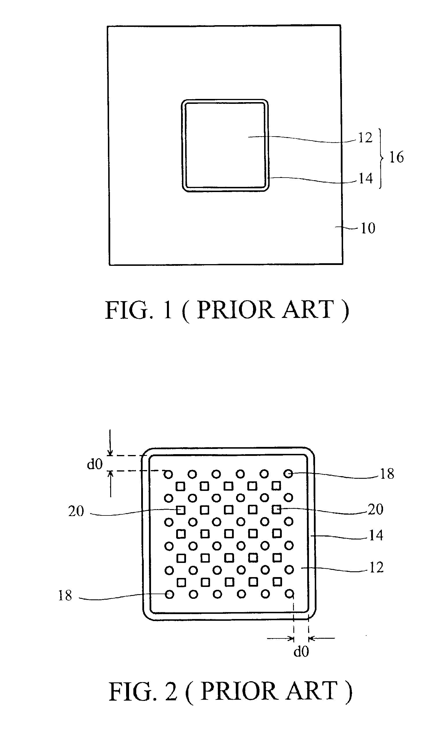
Die paddle for receiving an integrated circuit die in a plastic substrate
a technology of integrated circuits and dies, which is applied in the direction of solid-state devices, basic electric elements, electrical apparatus construction details, etc., can solve problems affecting package quality and reliability, and achieve the effect of eliminating delamination problems and improving package quality and reliability
- Summary
- Abstract
- Description
- Claims
- Application Information
AI Technical Summary
Benefits of technology
Problems solved by technology
Method used
Image


Examples
first embodiment
[First Embodiment]
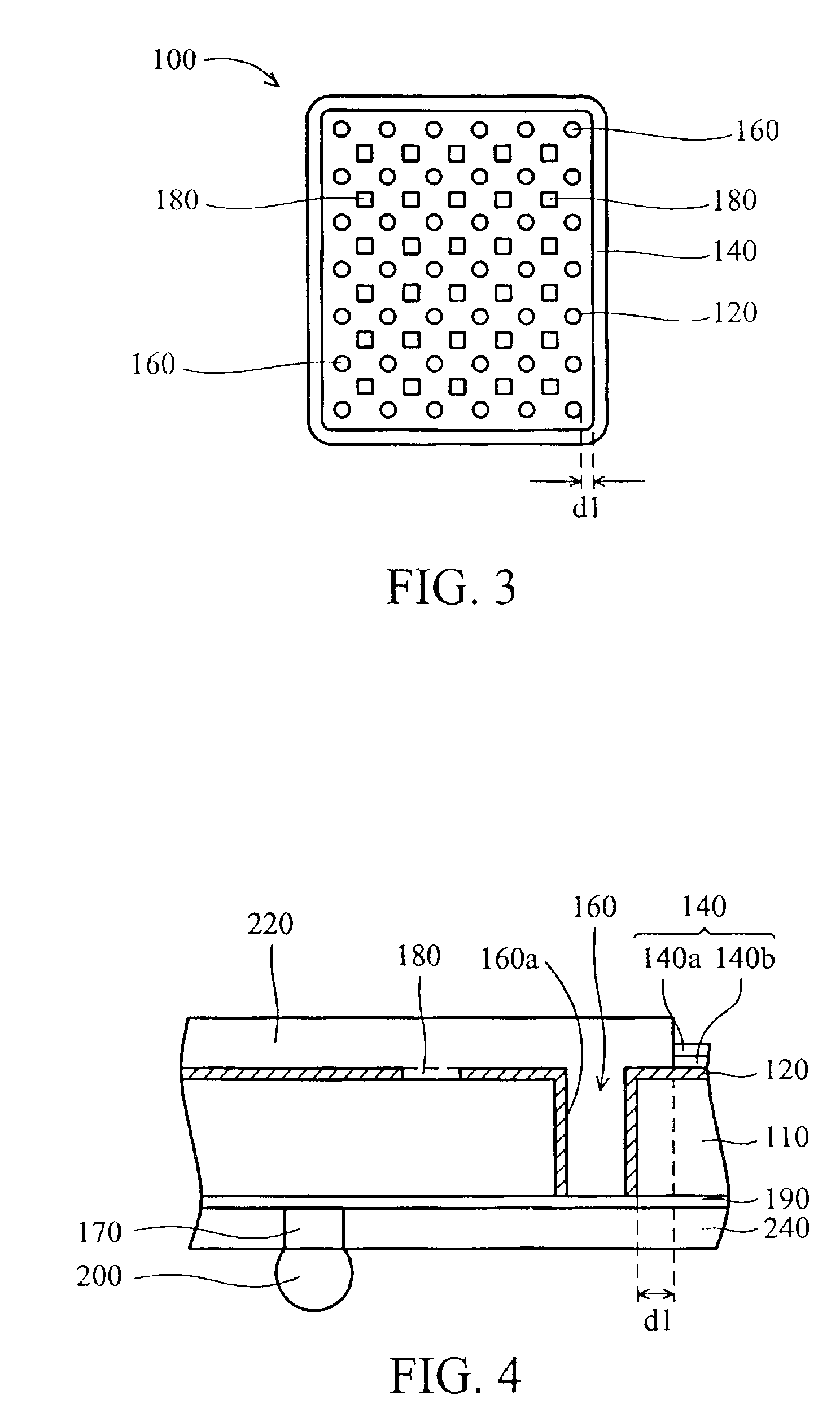
[0030]FIG. 3 and FIG. 4 show a square die paddle 100 in a plastic substrate 110 for receiving an integrated circuit die. The plastic substrate 110 is a plastic ball grid array substrate (PBGA substrate) and consists of epoxy resin.
[0031]The die paddle 100 includes a plurality of via holes 160, in an array arrangement, through the plastic substrate 110 and a copper film 120 attached to the central portion of the plastic substrate 110 and on the side walls 160a of the via holes 160 to electrically connect to the ground layer or the power layer. Also, the copper film 120 is formed on the plastic substrate 110 to define the die paddle region. In this embodiment, electrical signals can be transmitted from the integrate circuit die to the solder ball 200 through the copper film 120 in the via holes 160 and a conductive plug 170 in the solder resist 240.
[0032]The die paddle 100 further includes a plurality of openings 180, in an array arrangement, through the copper film ...
second embodiment
[Second Embodiment]
[0035]FIG. 5 and FIG. 6 show a square die paddle 300 in a plastic substrate 310 for receiving an integrated circuit die. The plastic substrate 310 is a plastic ball grid array substrate (PBGA substrate) and consists of epoxy resin.
[0036]The die paddle 300 includes a plurality of via holes 360, in an array arrangement, through the plastic substrate 310 and a copper film 320 attached to the central portion of the plastic substrate 310 and on the side walls 360a of the via holes 360 to electrically connect to the ground layer or the power layer. Also, the copper film 320 is formed on the plastic substrate 310 to define the die paddle region. In this embodiment, electrical signals can be transmitted from the integrate circuit die to the solder ball 400 through the copper film 320 in the via holes 360 and a conductive plug 370 in the solder resist 340.
[0037]The die paddle 300 further includes a plurality of openings 380, in an array arrangement, through the copper film...
PUM
 Abstract
Description
Claims
Application Information