Confocal 3D inspection system and process

a 3d inspection and process technology, applied in the direction of instruments, measurement devices, scientific instruments, etc., can solve the problems of general depth perception problems, shadowing problems, and current systems, devices, and methods that are either completely insufficient to handle these problems, or cannot meet the speed, accuracy, and other requirements

Inactive Publication Date: 2005-04-19
AUGUST TECH
View PDF35 Cites 14 Cited by
  • Summary
  • Abstract
  • Description
  • Claims
  • Application Information

AI Technical Summary

Benefits of technology

[0009]The inspecting of semiconductors or like substrates, and specifically the inspection of three dimensional surfaces or features, such as bumps, is accomplished by the present invention, which is a confocal sensor with a given depth response functioning using the principle of eliminating out of focus light thereby resulting in the sensor producing a signal only when the surface being inspected is in a narrow focal range. The result is an accurate height determination for a given point or area being inspected such that the accumulation of a plurality of height determinations from use of the confocal sensor system across a large surface allows the user to determine the topography thereof.
[0010]In sum, this system and process creates multiple parallel confocal optical paths whereby the out of focus light is eliminated by placing an aperture at a plane which is a conjugate focal plane to the surface of the sample. The result is that the sensor produces a signal only when the sample surface is in a narrow focal range.

Problems solved by technology

However, many obstacles exist as the significant height of bumps or the like causes focusing problems, shadowing problems, and just general depth perception problems.
Many of the current systems, devices, apparatus, and methods are either completely insufficient to handle these problems or cannot satisfy the speed, accuracy, and other requirements.

Method used


Image

  • Confocal 3D inspection system and process
  • Confocal 3D inspection system and process
  • Confocal 3D inspection system and process

Examples


Embodiment Construction

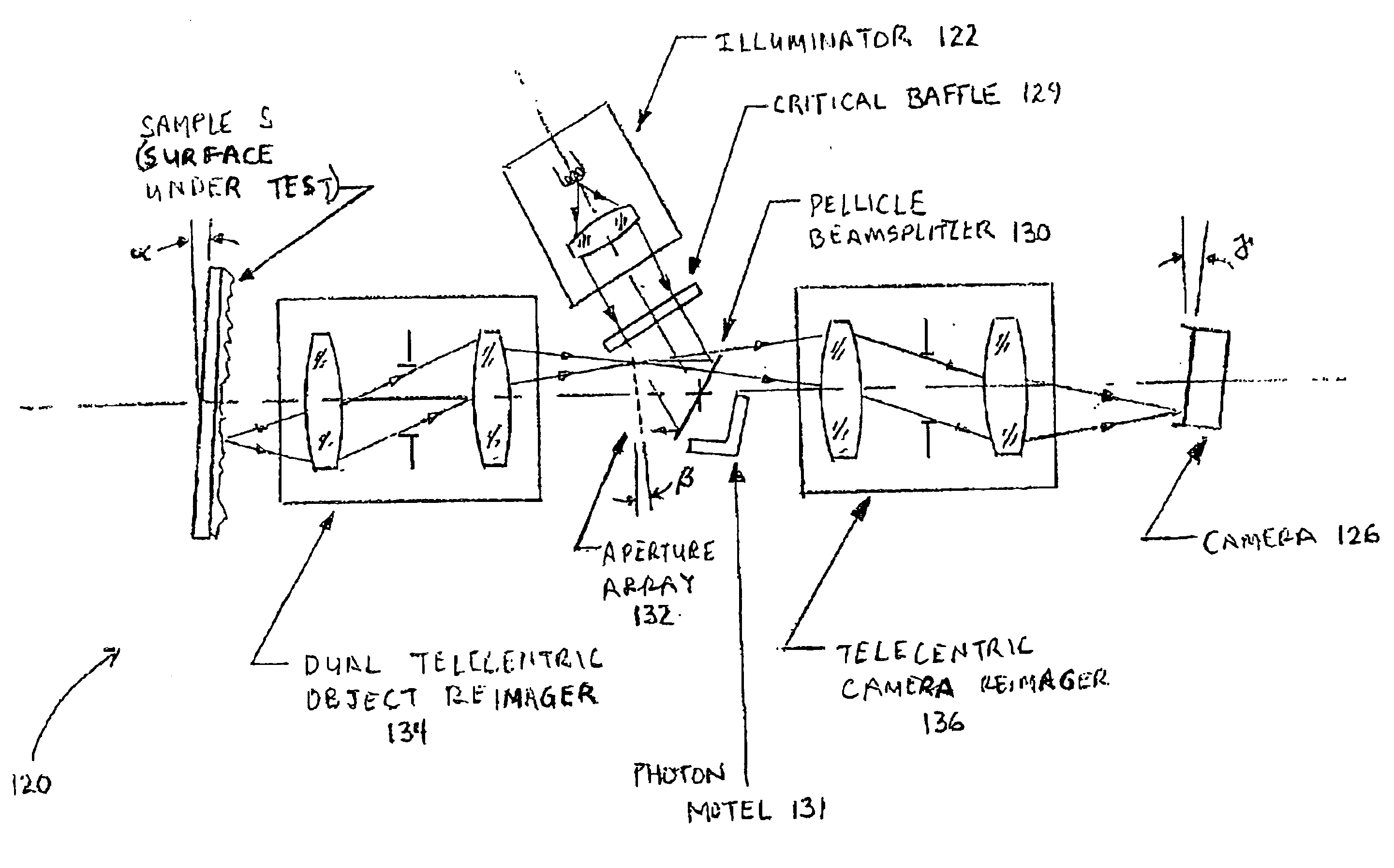
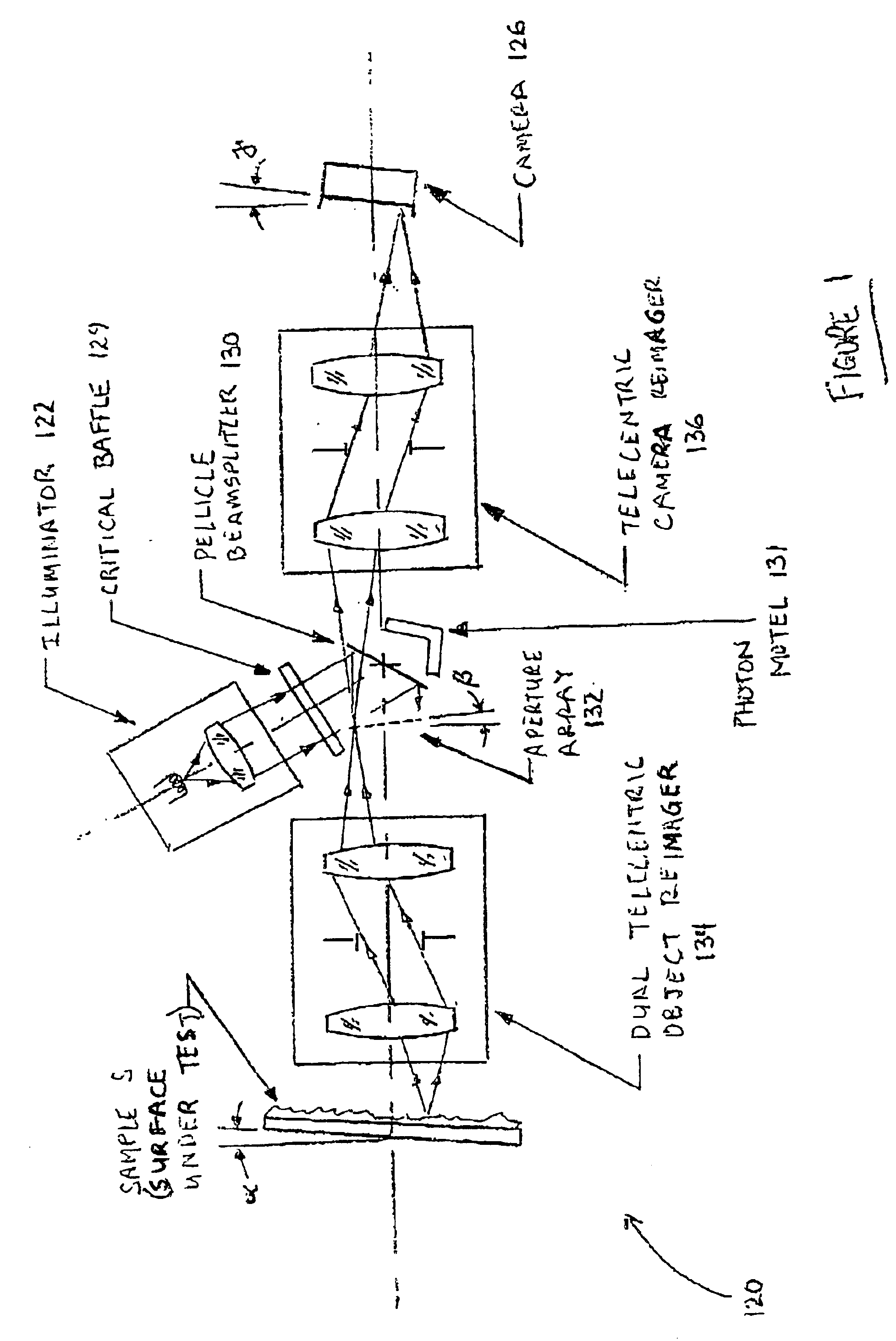
[0015]The three dimensional (3D) inspection system of the present invention is indicated generally at 120 as is best shown overall in FIG. 1 and is used in one environment to view, inspect, or otherwise optically measure three dimensional features or surfaces. One example is the measurement of bumps on wafers or like substrates. The 3D inspection system includes a light source 122, an optical subsystem 124, and a camera 126. The optical subsystem includes an intermediate focal assembly and a pair of imager or reimagers. The intermediate focal assembly in one embodiment includes an optional critical baffle 129, a beamsplitter 130, a photon motel 131, and an array mount including an aperture array 132, while the imager / reimagers in one embodiment include an object imager 134, and a camera reimager 136.

[0016]The light source 122 is any source of light that provides sufficient light to illuminate the sample S, and the light source may be positioned in any position so long as it provides...


PUM

PropertyMeasurementUnit
color temperatureaaaaaaaaaa
optical densityaaaaaaaaaa
anglesaaaaaaaaaa

Abstract

A confocal three dimensional inspection system, and process for use thereof, allows for rapid inspecting of bumps and other three dimensional (3D) features on wafers, other semiconductor substrates and other large format micro topographies. The sensor eliminates out of focus light using a confocal principal to create a narrow depth response in the micron range.

Description

CROSS REFERENCE TO RELATED APPLICATIONS[0001]This application claims priority to the following provisional patent application filed on Jul. 16, 2001: U.S. Ser. No. 60 / 305,823, Applicant expressly requests that this application never be published or otherwise disclosed to the public unless it issues as a U.S. Patent, and Applicant expressly acknowledges that it may not be filed outside of the U.S.BACKGROUND OF THE INVENTION[0002]1. Technical Field[0003]The present invention relates to a system, and process for use thereof, for inspecting wafers and other semiconductor or microelectronic substrates, and specifically for inspecting three dimensional (3D) surfaces or features thereon such as bumps. Specifically, the present invention relates to a confocal optical system for inspecting bumps and other 3D features on wafers or like substrates, and a process of using such system.[0004]2. Background Information[0005]Over the past several decades, the microelectronics and semiconductor has e...

Claims


Application Information

Patent Timeline
Patent Type & Authority Patents(United States)
IPC IPC(8): G01N21/00G01N21/956G02B21/00G02B21/22
CPCG01N21/956G02B21/22G02B21/0016
Inventor WATKINS, CORYVAUGHN, DAVID
Owner AUGUST TECH
Why Eureka
Try Eureka