
Nanowire optoelectric switching device and method

Inactive Publication Date: 2005-04-19
RGT UNIV OF CALIFORNIA
View PDF4 Cites 55 Cited by
  • Summary
  • Abstract
  • Description
  • Claims
  • Application Information

AI Technical Summary

Benefits of technology

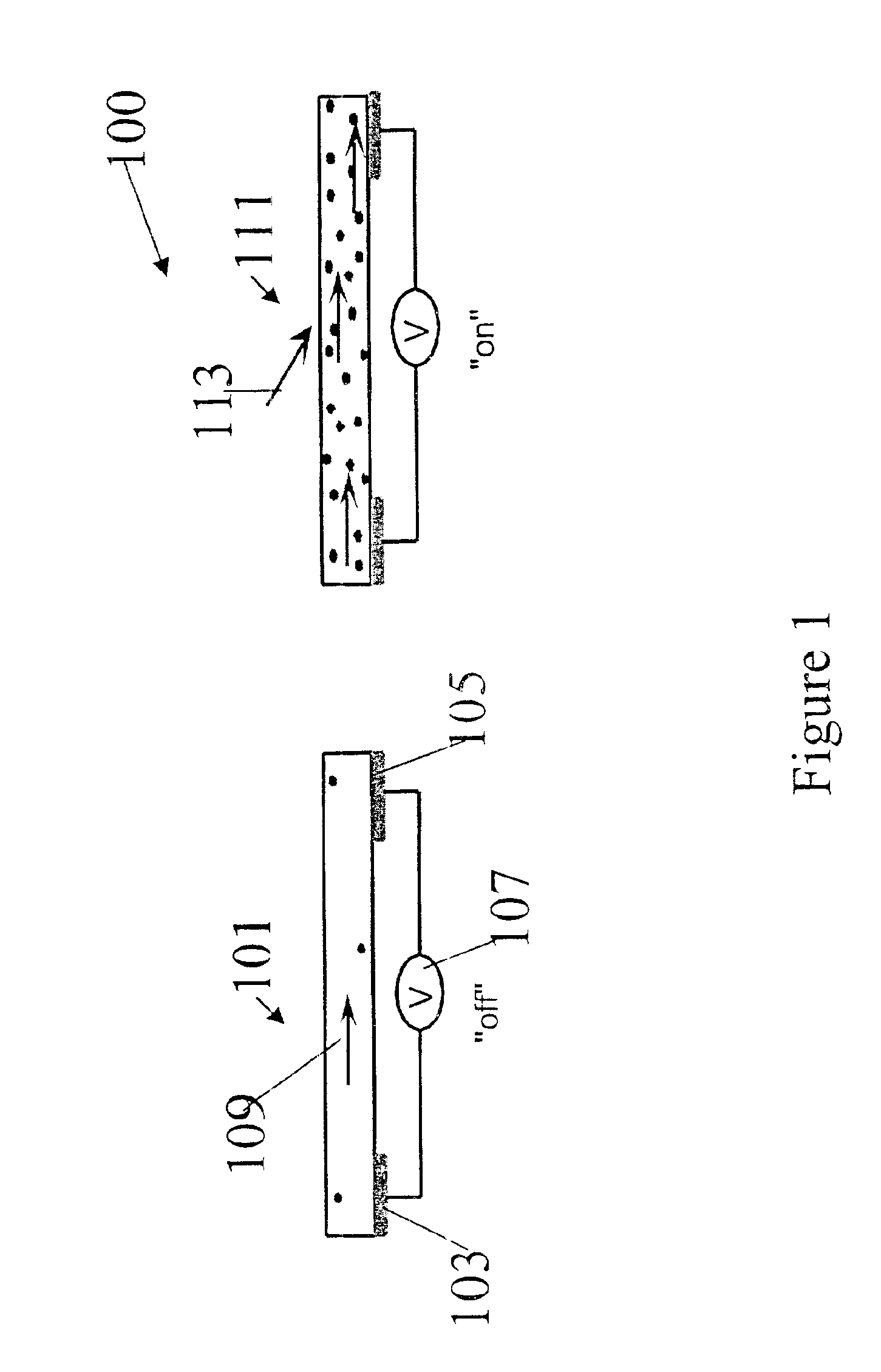
[0009]In an alternative specific embodiment, the invention provides a nanowire opto-electronic switching device. The device has a nanowire structure comprising an elongated member having a cross-sectional diameter ranging from about 1 nanometers but less than about 500 nanometers. Alternatively, the nanowire structure can have other dimensions. The device also has a first terminal coupled to a first portion of the nanowire structure and a second terminal coupled to a second portion of the nanowire structure. The second portion of the nanowire structure is disposed spatially from the first portion of the nanowire structure. An active surface structure is coupled to the nanowire structure. The active surface structure extends from the first portion to the second portion along the elongated member. The nanowire structure has a first resistance value as measured between the first terminal and the second terminal while the active surface is subjected to a first level of electromagnetic radiation. The nanowire structure has a sec

Problems solved by technology

The Noyce patent, however, is limited to conventional ways of manufacturing and operating semiconductor integrated circuits.
Although there has been some work in manufacturing and using nanowires, such work has been limited.

Method used


Image

  • Nanowire optoelectric switching device and method
  • Nanowire optoelectric switching device and method
  • Nanowire optoelectric switching device and method

Examples


examples

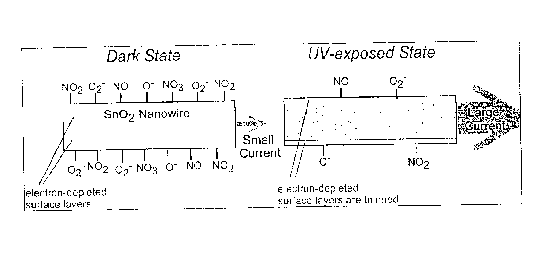
[0054]To prove the principle and operation of the present invention, we performed experiments. These experiments were merely examples and should not unduly limit the scope of the inventions defined by the claims herein. One of ordinary skill in the art would recognize many other variations, modifications, and alternatives. As we will demonstrate, highly sensitive ultraviolet optical sensors based on individual zinc oxide nanowires were demonstrated. Upon exposure to ultraviolet light, electrical resistivity of the semiconducting nanowires was found to decrease by 4 to 6 orders of magnitude. This transition serves as the basis for nanowire opto-electronic binary switches, which exhibit high sensitivity, selectivity and excellent reversibility at room temperature. Such nanowire devices may also have implications in single photon detection, as well as in chemical and biological sensors.

[0055]We have demonstrated that nanowires and nanotubes could be ideal building blocks for nanoscale ...


PUM


Abstract

A nanowire switching device and method. The device has a nanowire structure comprising an elongated member having a cross-sectional area ranging from about 1 nanometers but less than about 500 nanometers, but can also be at other dimensions, which vary or are substantially constant or any combination of these. The device also has a first terminal coupled to a first portion of the nanowire structure; and a second terminal coupled to a second portion of the nanowire structure. The second portion of the nanowire structure is disposed spatially from the first portion of the nanowire structure. An active surface structure is coupled to the nanowire structure. The active surface structure extends from the first portion to the second portion along the elongated member.

Description

STATEMENT AS TO RIGHTS TO INVENTIONS MADE UNDER FEDERALLY SPONSORED RESEARCH OR DEVELOPMENT[0001]This invention was made with Government support under Grant No. NSF DMR0092086 Awarded by the National Science Foundation. The Government has certain rights to this invention.BACKGROUND OF THE INVENTION[0002]The present invention generally relates to a nanowire optoelectric switching structure and method. More particularly, the invention provides a device and method for switching a signal using a nanowire via electro-optic means. Merely by way of example, the invention is applied to switching electrical signals of a switching device. But it would be recognized that the invention has a much wider range of applicability. For example, the invention can be applied to other types of switching devices, such as chemical detectors, sensors, MEMS, MOEMS, biostructures, photodetectors, humidity sensors, and the like.[0003]Through the years, many techniques have been developed to carry signals thro...

Claims


Application Information

Patent Timeline
IPC IPC(8): H01L51/05H01L51/30G02B6/35G11C13/02H01H1/02
CPCB82Y10/00G11C13/025Y10S977/932G11C2213/16G11C13/04
Inventor YANG, PEIDONGKIND, HANNESYAN, HAOQUANLAW, MATTHEWMESSER, BENJAMIN
Owner RGT UNIV OF CALIFORNIA
Learn More