Susceptor of apparatus for manufacturing semiconductor device

a semiconductor device and apparatus technology, applied in the direction of electrolysis components, vacuum evaporation coatings, coatings, etc., can solve the problems of inability to operate normally, poor properties of thin films to be deposited or patterned, and inability to meet the requirements of manufacturing process,

Inactive Publication Date: 2005-04-26
JUSUNG ENG
View PDF8 Cites 375 Cited by
  • Summary
  • Abstract
  • Description
  • Claims
  • Application Information

AI Technical Summary

Benefits of technology

[0020]An advantage of the present invention is to provide a susceptor of an apparatus for manufacturing a semiconductor device that prevents a heater therein from being oxidized.
[0021]Additional features and advantages of the invention will be set forth in the description which follows, and in part will be apparent from the description, or may be learned by practice of the invention. The objectives and other advantages of the invention will be realized and attained by the structure particularly pointed out in the written description and claims hereof as well as the appended drawings.
[0022]To achieve these and other advantages and in accordance with the purpose of the present invention, as embodied and broadly described, a susceptor of an apparatus for manufacturing a semiconductor device includes

Problems solved by technology

The thin film to be deposited or to be patterned has bad properties.
Moreover, if the heater34 is oxidize

Method used


Image

  • Susceptor of apparatus for manufacturing semiconductor device
  • Susceptor of apparatus for manufacturing semiconductor device
  • Susceptor of apparatus for manufacturing semiconductor device

Examples


Embodiment Construction

[0033]Reference will now be made in detail to the illustrated embodiment of the present invention, which is illustrated in the accompanying drawings.

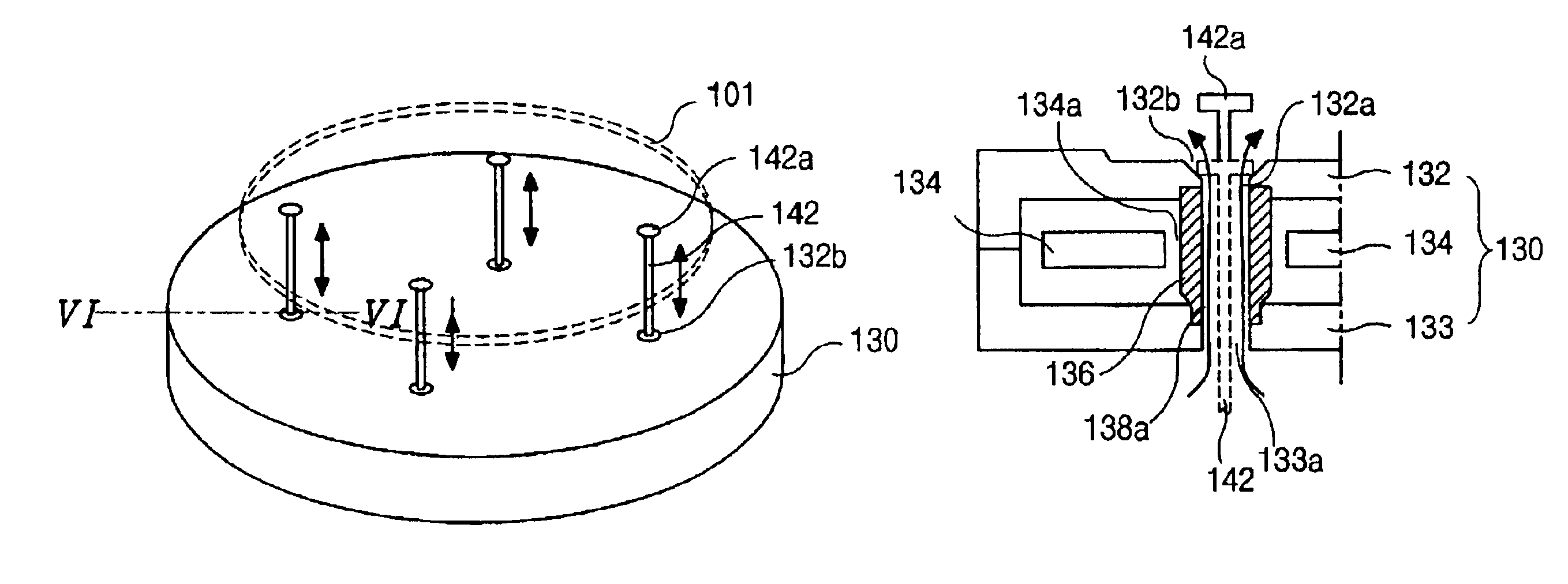
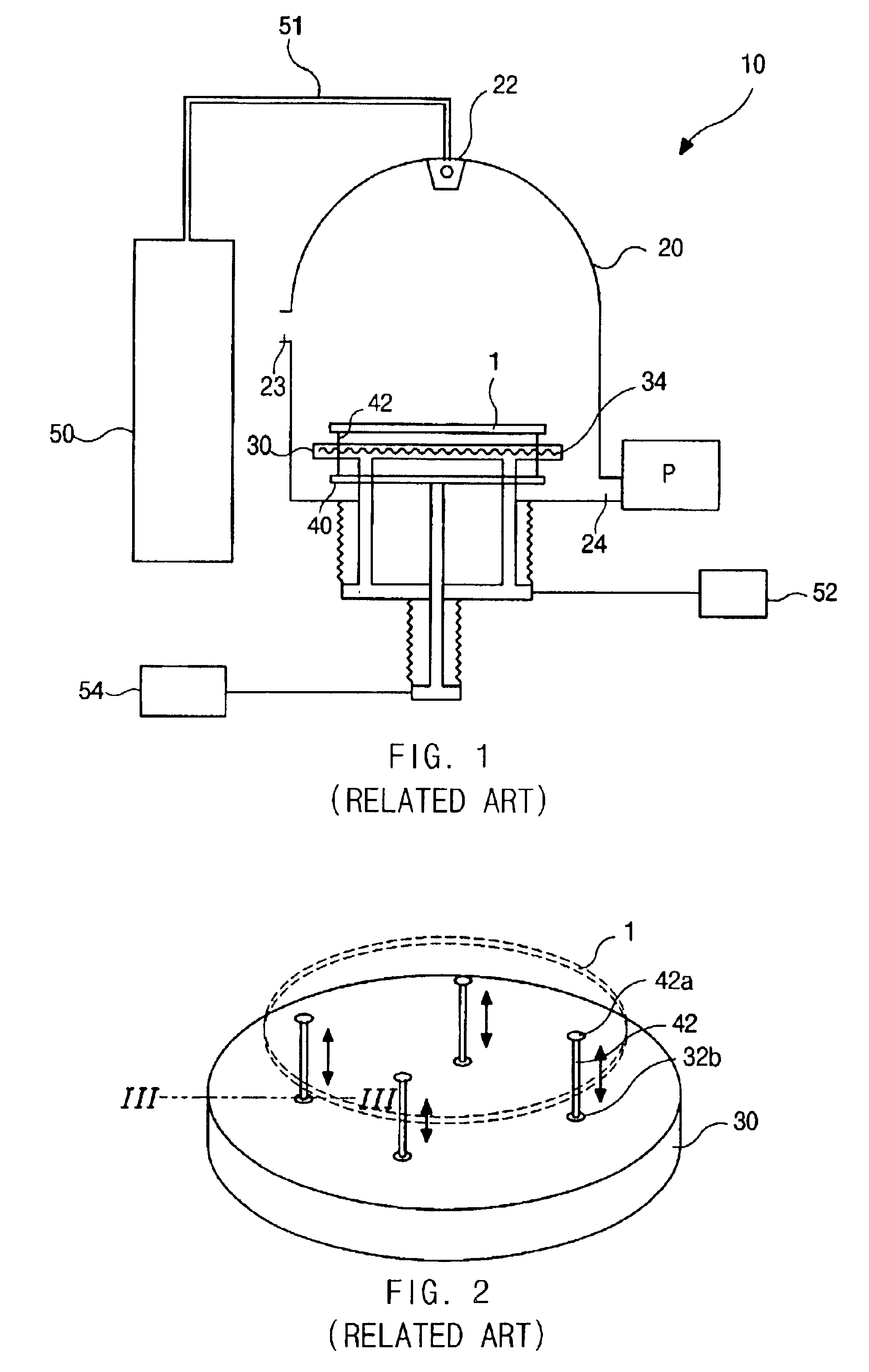
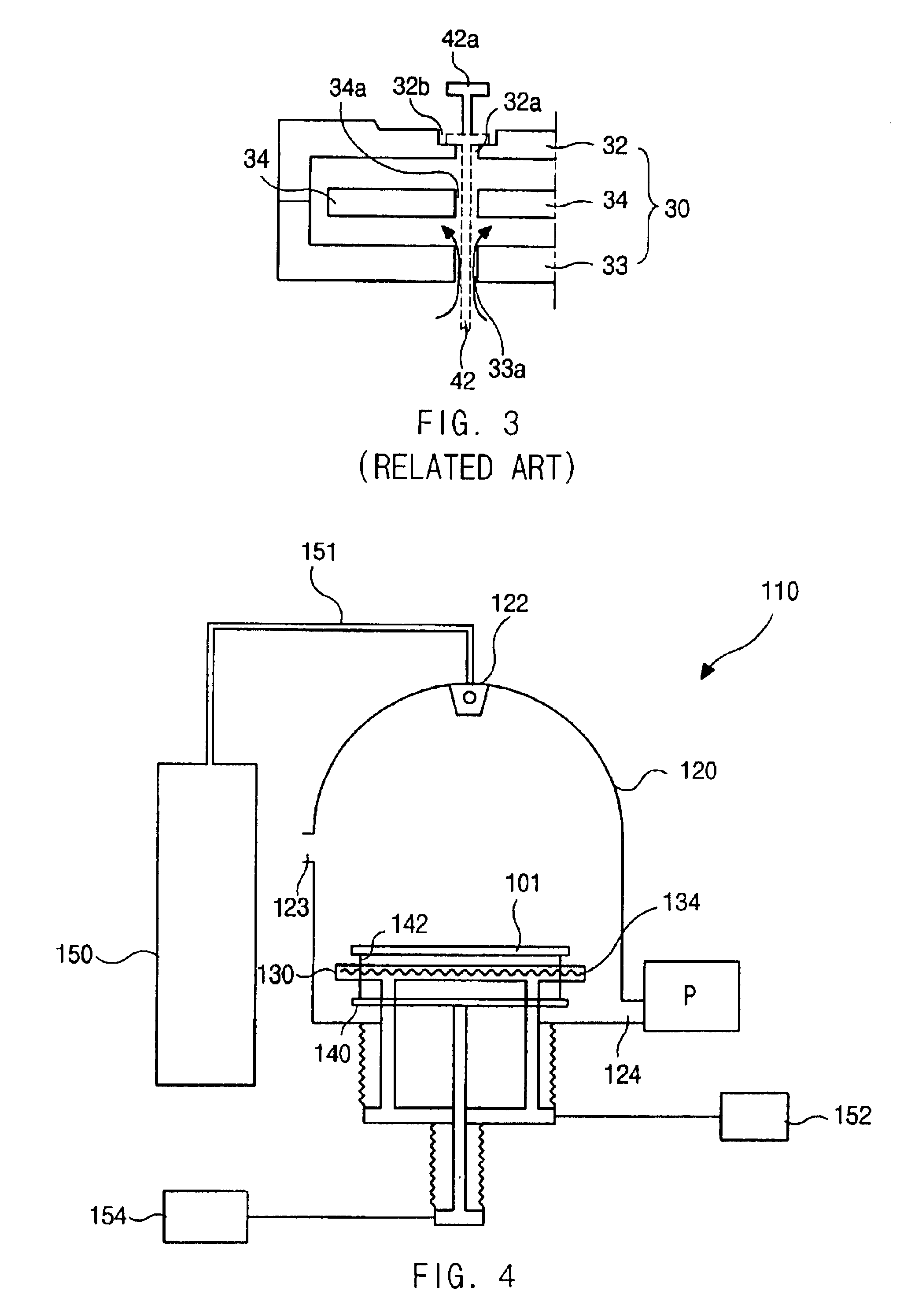
[0034]FIG. 4 shows an apparatus for manufacturing a semiconductor device according to an embodiment of the present invention. In FIG. 4, the apparatus 110 includes a chamber 120 and a supplying part 150. The chamber 120 is an airtight reaction container, and in the chamber 120, a substrate 101 such as a silicon wafer to be handled is disposed. Thus, a process that a thin film is deposited on the substrate 101 or a thin film formed on the substrate 101 is patterned is accomplished in the chamber 120. The supplying part 150 stores and supplies source materials and reaction materials to the chamber 120.

[0035]The chamber 120 has an inlet 123, an outlet 124, an injector 122, and a susceptor 130. The upper part of the chamber 120 may be dome-shaped. The inlet 123 is formed in a wall of the chamber 120, and the substrate 101 to be handled come...


PUM

PropertyMeasurementUnit
Diameteraaaaaaaaaa

Abstract

A susceptor of an apparatus for manufacturing a semiconductor device includes a first part having a first lift pin hole, a second part combined with the first part and forming a space with the first part, wherein the second part has a second lift pin hole corresponding to the first lift pin hole, a heater disposed in the space, wherein the heater has a third lift pin hole corresponding to the first and second lift pin holes, a lift pin tube inserted in the first, second and third lift pin holes, wherein the lift pin tube is combined with the first and second part thereby preventing air from going into the space, and a lift pin passing through the lift pin tube.

Description

[0001]The present invention claims the benefit of Korean Patent Application No. 2001-70222, filed on Nov. 12, 2001 in Korea, which is hereby incorporated by reference for all purposes as if fully set forth herein.BACKGROUND OF THE INVENTION[0002]1. Field of the Invention[0003]The present invention relates to an apparatus for manufacturing a semiconductor device and more particularly, to a susceptor of an apparatus for manufacturing a semiconductor device.[0004]2. Discussion of the Related Art[0005]A development for a new material has been actively performed in the field and diverse large-scale integrated circuits (LSI) such as ultra large-scale integrated circuits (ULSI) have been developed due to a rapid growth of the new material development. That is, because the new material for forming thin films such as an insulating layer, a semiconductor layer and a conductive layer, which constitute a semiconductor device, has been widely developed in the field, the large-scale integrated ci...

Claims


Application Information

Patent Timeline
IPC IPC(8): C23C16/00C23F1/00C23C14/00H01L21/302H01L21/68H01L21/02H01L21/67C23C16/458H01L21/00H01L21/687
CPCC23C16/4581H01L21/68742H01L21/67109C23C16/4586H01L21/68
Inventor KIM, YONG-JIN
Owner JUSUNG ENG
Why Eureka
Try Eureka