

Biaxially textured composite substrates
a composite substrate and biaxial texture technology, applied in the direction of superimposed coating process, superconducting magnet/coil, magnetic body, etc., can solve the problems of system drawbacks that detract from the viability of the system, and the slow deposition of the ysz layer is considered too slow for commercial production
- Summary
- Abstract
- Description
- Claims
- Application Information
AI Technical Summary
Benefits of technology
Problems solved by technology
Method used
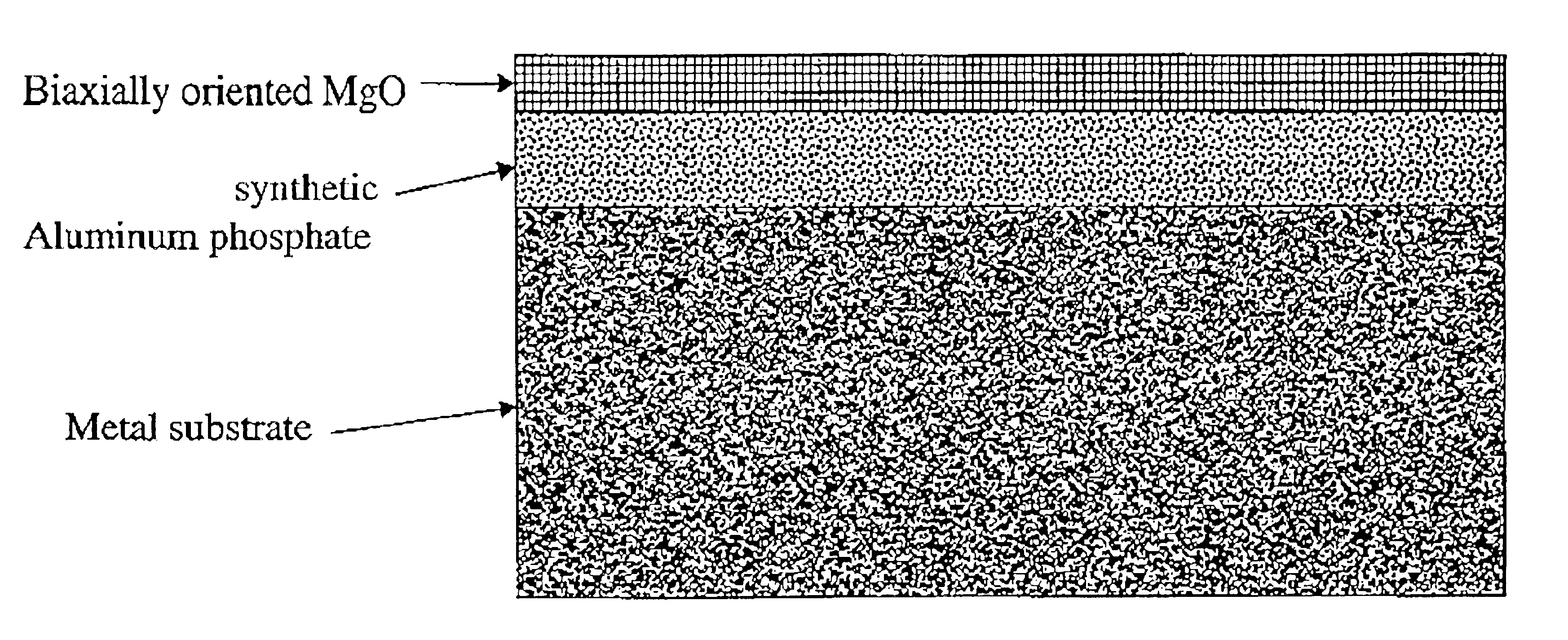
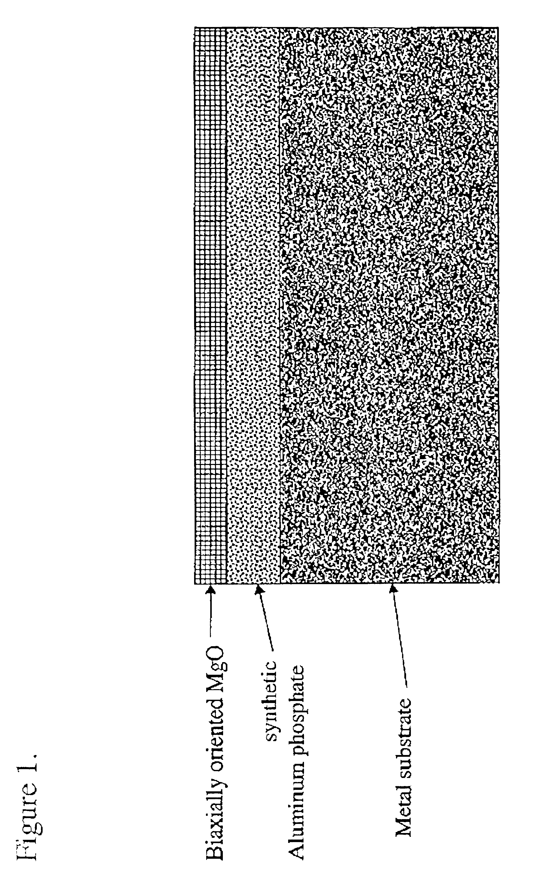
Image

Examples
example 1
[0031]On a nickel alloy substrate (Hastelloy C276), was deposited by dip coating a layer of aluminum phosphate about 200 nanometers in thickness. The substrates had been ultrasonically cleaned in soap and water, rinsed with deionized water, rinsed with methanol, blown dry with filtered nitrogen, and mechanically polished to a smoothness (RMS roughness) of about 2 nm. After dipping, the aluminum phosphate layer was annealed by heating at above 750° C. for about 1 hour. Onto this resultant article of nickel alloy substrate and aluminum phosphate was deposited a layer of MgO at room temperature by ion-assisted, electron beam evaporation system similar to that of Wang et al., App. Phys. Lett., v. 71, no. 20, pp. 2955-2957 (1997). The ion source was manufactured by Ion Tech, Inc. (Ft. Collins, Colo.) with a source geometry of 22 cm by 2.5 cm. The substrate normal to ion-assist beam angle was 45±3°. The ion source gas was argon. The ion source gas was introduced to a background partial pr...
PUM
| Property | Measurement | Unit |
|---|---|---|
| thickness | aaaaa | aaaaa |
| transport critical current | aaaaa | aaaaa |
| RMS roughness | aaaaa | aaaaa |
Abstract
Description
Claims
Application Information