Radiation detector

a detector and radiation technology, applied in the field of radiation detectors, can solve the problems of end edge portion, detector cannot operate in normal operation, and the probability of causing discharge breakdown is rapidly increased, and achieve the effect of stable detecting operation

Inactive Publication Date: 2005-04-26
SHIMADZU CORP
View PDF3 Cites 17 Cited by
  • Summary
  • Abstract
  • Description
  • Claims
  • Application Information

AI Technical Summary

Benefits of technology

[0013]The invention has been created in order to resolve the problem by concentration of an electric field on an end edge portion of an electrode. It is an object thereof to provide a radiation detector capable of preventing penetration discharge or creeping discharge by concentration of an electric field on an end edge portion of a voltage application electrode formed at a surface of a radiation sensitive type semiconductor film and capable of guaranteeing stable detecting operation for a long period of time.
[0028]Further, in the case of the radiation detector of the first aspect of the present invention, the insulating substance with the high withstand voltage property is formed between the semiconductor thick film and the end edge portion of the voltage application electrode. Therefore, as is predicted also from a result of an electric field calculating simulation of FIG. 10, concentration of an electric field on the end edge portion of the voltage application electrode is prevented, a prestage phenomenon of penetration discharge or discharge breakdown is not caused and stable detecting operation is continued for a long period of time.
[0029]Further, in the case of the radiation detector of the second aspect of the present invention, the high resistance film, which is provided with a solvent resistance property and a carrier selective property, is formed at least between the semiconductor thick film and the insulating substance with the high withstand voltage property. Therefore, there is not caused a phenomenon in which the surface of the semiconductor thick film is denatured by a solvent component of the high withstand voltage insulating substance, creeping discharge is caused and withstand voltage is lowered. Further, when a carrier selective material suitable for use is pertinently selected, a deterioration in sensitivity, an increase in dark current or the like at a portion of forming the high resistance film is prevented.
[0031]In the case of the radiation detector of the fourth aspect of the present invention, the withstand voltage insulating substance has the thickness with the gradient so that the insulating substance is formed to be infinitely thinned to the inner side and thickened to the outer side. Therefore, concentration of the electric field on the end edge portion of the voltage application electrode is further reduced and further stable detecting operation is guaranteed for a long period of time.

Problems solved by technology

However, according to the related art radiation detector, there is a problem that an electric field is concentrated on an end edge portion of the voltage application electrode 82 formed at the surface of the amorphous semiconductor thick film 81 and dielectric breakdown is liable to cause at the end edge portion.
Further, these noises spread also to other portion and the detector cannot operate in the normal operation.
Further, when the high bias voltage is continued to apply to the voltage application electrode for a long period of time, a probability of causing discharge breakdown is rapidly increased.

Method used


Image

  • Radiation detector
  • Radiation detector
  • Radiation detector

Examples


first embodiment

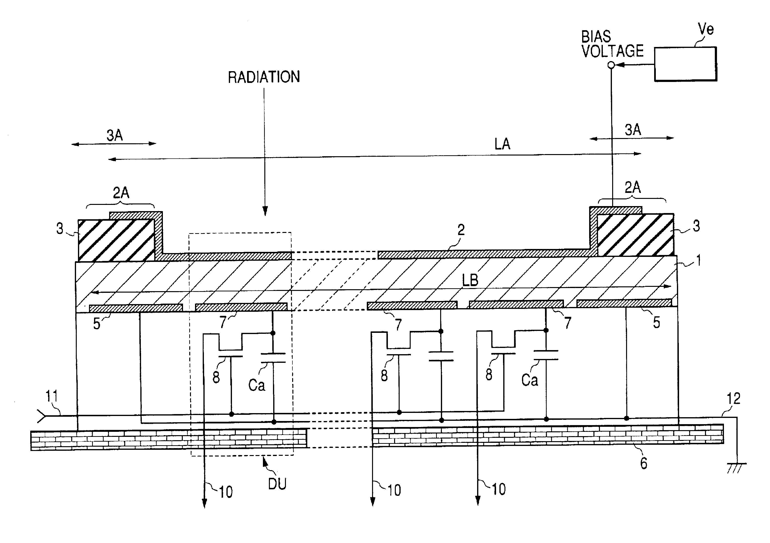
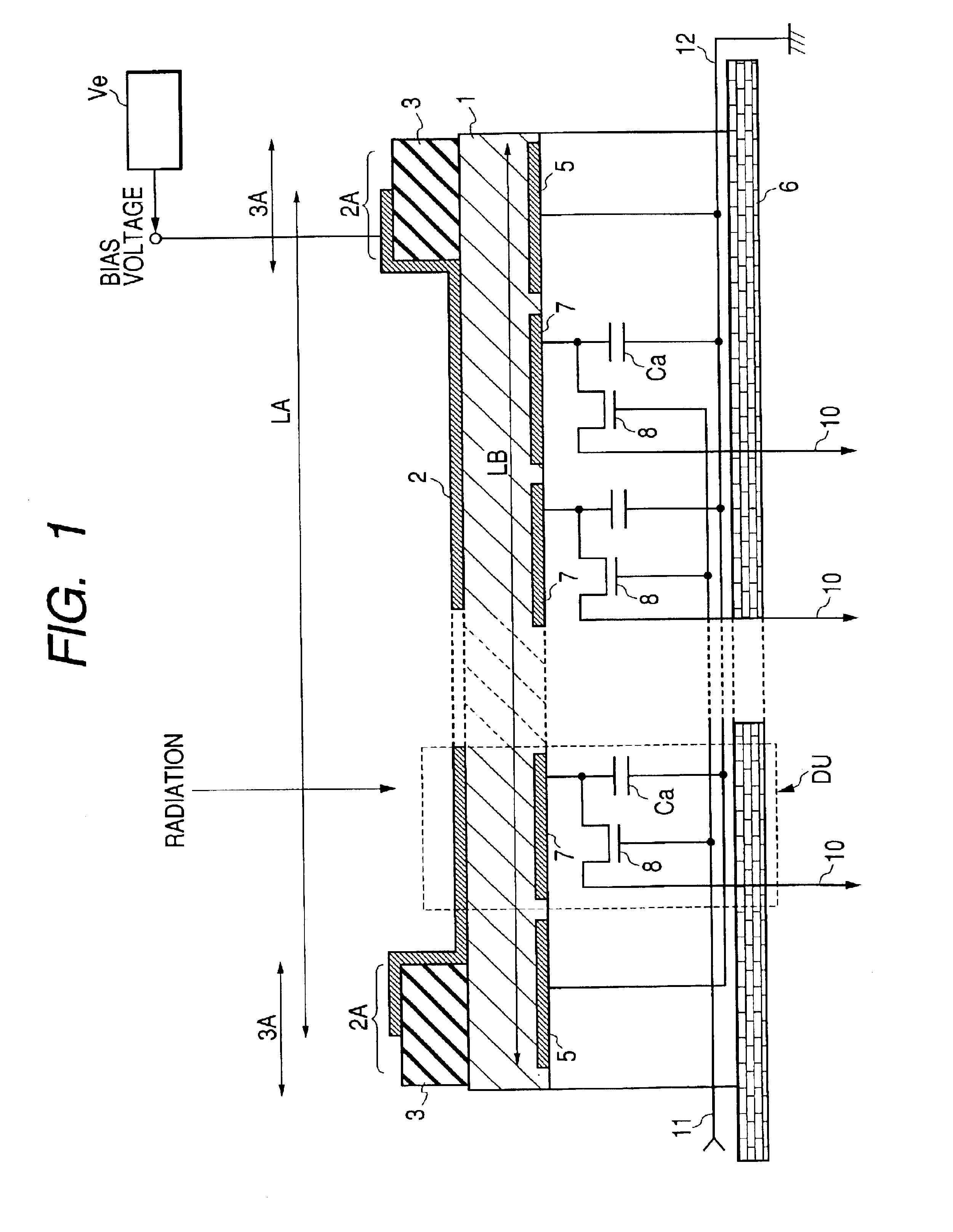
[0046]As shown in FIG. 1, a radiation detector of the first embodiment includes an insulating substrate 6 of a glass substrate or the like, an amorphous semiconductor thick film 1, and a voltage application electrode 2, which serve as a radiation sensor portion. The insulating substrate 6 is formed with a capacitor Ca comprising SiO2 layer or the like and a switching element 8, for example, a transistor (TFT), which is brought into a normally OFF (cut) state, for outputting charge stored at the capacitor Ca. The amorphous semiconductor thick film 1 is electrically connected to the charge storage capacitor Ca and formed above the insulating substrate 6 via a carrier collection electrode 7. In the amorphous semiconductor thick film 1, charge transfer media (carriers) are generated by incidence of radiation. The voltage application electrode 2 is provided at a surface of the amorphous semiconductor thick film 1 which is a radiation incident side.

[0047]The radiation detector of the firs...

second embodiment

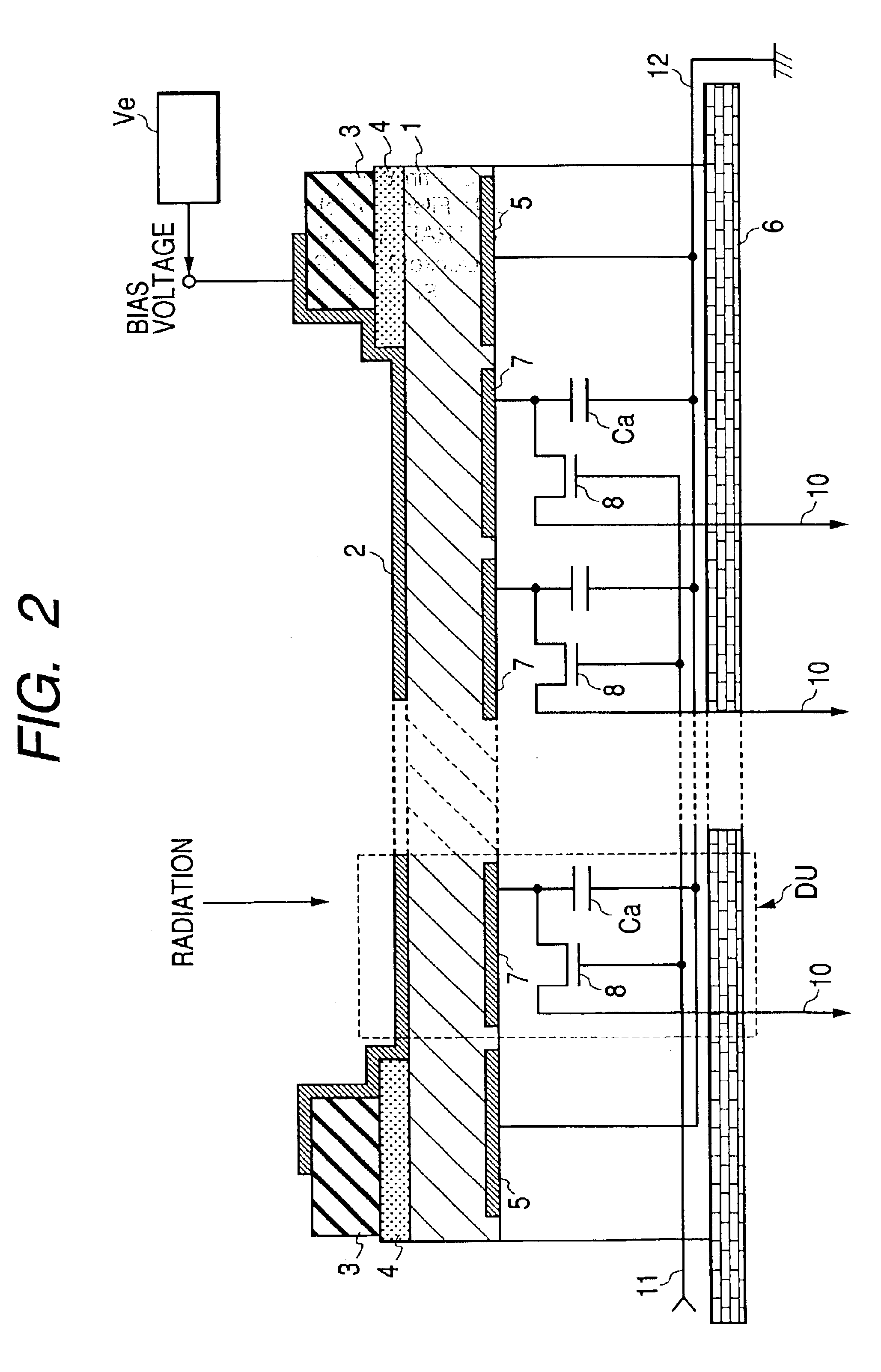
[0051]Further, shown in FIG. 2, an Sb2S3 film which is a high resistance film 4 which is provided with the solvent resistance property and the carrier selective property, is formed by a thickness of about 1 μm at least between the amorphous semiconductor thick film 1 and the insulating substance 3 with the high withstand voltage property. Although the Sb2S3 film is pointed out as an example of the high resistance film 4 which is provided with the solvent resistance property and the carrier selective property, other than Sb2S3, an inorganic semiconductor film of CdS, AsSe, SeTe, CdTe or the like and an organic film material of polycarbonate or the like added with a carrier transfer material, can be used. Although film thicknesses of these differ by selectivity of carrier, solvent resistance property, or adherence to the amorphous semiconductor thick film 1, the film thicknesses can be selected in a range of 0.05 μm through 10 μm. Further, although as the carrier selective high resis...

third embodiment

[0062]Next, an explanation will be given of a method of forming the radiation sensor portion by taking an example of the case of the third embodiment shown in FIG. 3. First, the thin film transistor for the switching element 8, the capacitor Ca and the carrier collection electrode 7 are formed on the surface of the insulating substrate 6 by utilizing a thin film forming technique by a vacuum film forming process and a patterning technique by a photolithography process. Next, the amorphous semiconductor thick film 1, the carrier selective high resistance film 4, the high withstand voltage insulating substance 3 and the voltage application electrode 2 are laminated successively on the insulating substrate 6, so that the radiation sensor portion is finished.

[0063]Here, as the high withstand voltage insulating substance 3, silicone resin can be used. In such a case, there is used a material in which the viscosity of the high withstand voltage insulating silicone resin is adjusted by usi...


PUM


Abstract

A high withstand voltage insulating substance is formed between a radiation sensitive type amorphous semiconductor thick film suitable for forming a large area and an end edge portion of a voltage application electrode. As a result, concentration of an electric field on the end edge portion of the voltage application electrode is eliminated and a prestage phenomenon of penetration discharge or discharge breakdown is not caused.

Description

BACKGROUND OF THE INVENTION[0001]1. Field of the Invention[0002]The present invention relates to a radiation detector of a direct conversion type used in the medical field, the industrial field, the atomic field and the like, particularly relates to a technique for improving a withstand voltage property of a semiconductor film of a radiation sensitive type.[0003]2. Description of the Related Art[0004]According to detectors for detecting radiation (for example, X-ray), there are an indirect conversion type detector and a direct conversion type detector. The indirect conversion type detector is adapted to convert radiation (for example, X-ray) firstly into light and thereafter convert converted light into an electric signal by photoelectric conversion. The direct conversion type detector is adapted to directly convert incident radiation into an electric signal by a semiconductor film of a radiation sensitive type.[0005]The latter direct conversion type detector is constructed by a con...

Claims


Application Information

Patent Timeline
Patent Type & Authority Patents(United States)
IPC IPC(8): H01L27/146H01L27/14G01T1/24H01L31/09H04N5/30H04N5/335H04N5/369H04N5/374
CPCH01L27/14676H01L27/14609G01T1/24
Inventor SATO, KENJITOKUDA, SATOSHI
Owner SHIMADZU CORP
Why Eureka
Try Eureka