Deep trench isolation of embedded DRAM for improved latch-up immunity

a technology of embedded dram and deep trench isolation, which is applied in the direction of semiconductor devices, electrical equipment, transistors, etc., can solve the problems of constant need to increase the density of devices, damage to cmos devices, and failure of devices if not addressed

Inactive Publication Date: 2005-04-26
ELPIS TECH INC
View PDF16 Cites 48 Cited by
  • Summary
  • Abstract
  • Description
  • Claims
  • Application Information

AI Technical Summary

Benefits of technology

[0006]The above discussed and other drawbacks and deficiencies of the prior art are overcome or alleviated by a protective structure for blocking the propagation of defects generated in a semiconductor device. In an exemplary embodiment, the structure includes a deep trench isolation formed between a memory storage region of the semiconductor device and a logic circuit region of the semiconductor device, the deep trench isolation being filled with an insulative material. The deep trench isolation thereby prevents the propagation of crystal defects generated in the logic circuit region from propagating into the memory storage region.

Problems solved by technology

Moreover, as integrated semiconductor devices continue to grow in complexity, there is a constant need to increase the density of the devices.
This increase in density can create several problems, particularly with eDRAM devices, that can lead to device failure if not addressed.
One such problem stems from the propensity for some semiconductor devices, such as those included in CMOS circuitry, to “latch-up.” Latch-up is a well known problem triggered by certain electrical conditions acting upon unwanted parasitic bipolar transistors contained in the device structure.
This large current creates excessive heat which can subsequently damage the CMOS device.
However, as a result of these high dose / high energy implants, crystal defects may be generated in the implantation (CMOS) area and propagated relatively long distances, possibly even into a neighboring array of embedded DRAM storage cells.
The propagated defects, in turn, can increase the junction leakage of the less tolerant DRAM cells and thereby negatively impact the data retention time of those cells.

Method used


Image

  • Deep trench isolation of embedded DRAM for improved latch-up immunity
  • Deep trench isolation of embedded DRAM for improved latch-up immunity
  • Deep trench isolation of embedded DRAM for improved latch-up immunity

Examples


Embodiment Construction

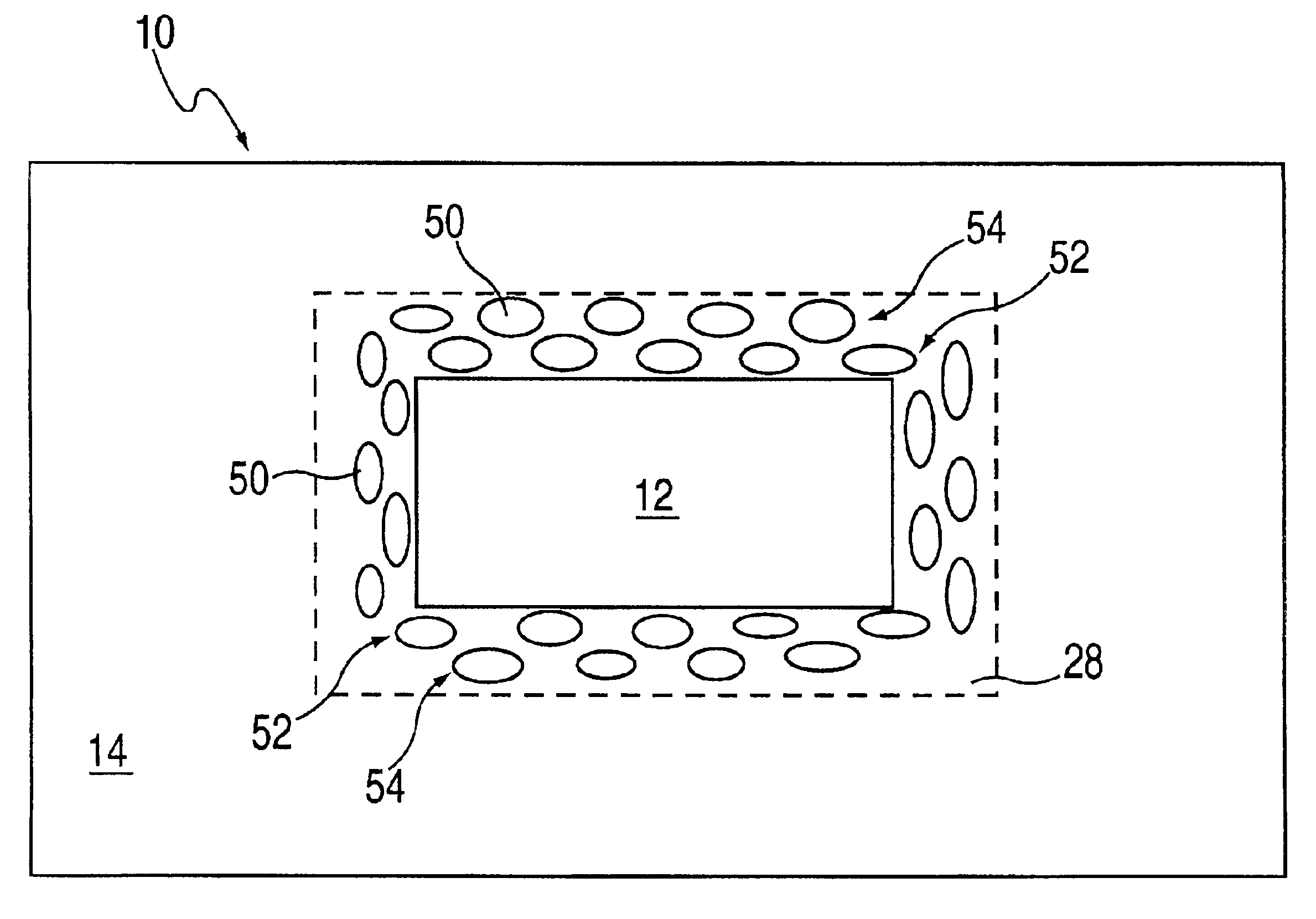
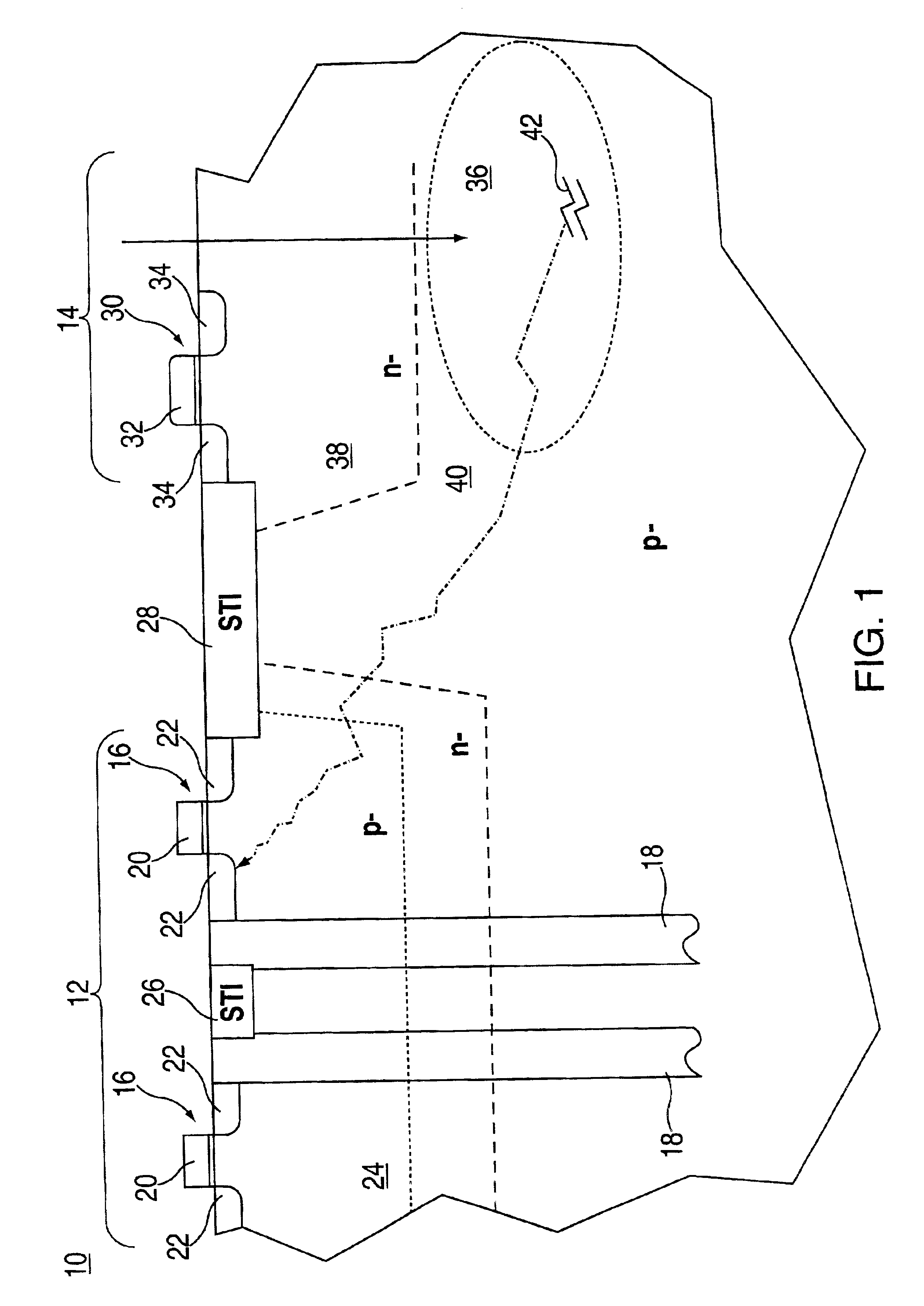
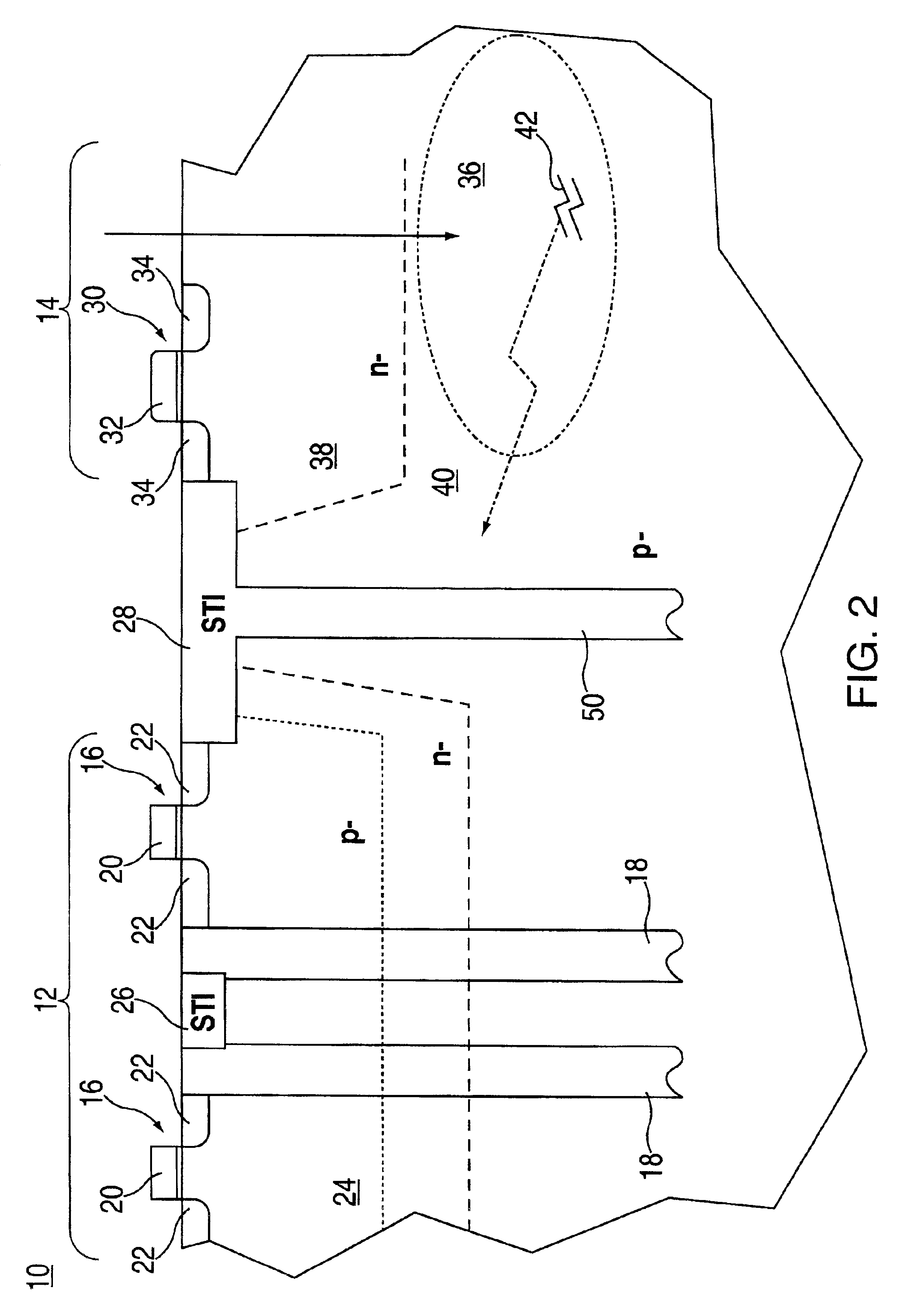
[0013]Referring initially to FIG. 1, there is shown a cross sectional view of an existing embedded DRAM (eDRAM) device 10. The eDRAM device 10 includes a DRAM array region 12 (in which an array of individual DRAM storage cells are configured), as well as a logic circuit region 14 in which various logic circuitry is located. Generally speaking, the DRAM array region 12 includes a number of individual DRAM storage cells each having an access transistor 16 and a trench storage capacitor 18. The access transistors 16 further include a gate 20, as well as source / drain diffusion areas 22. In the example illustrated, diffusion areas 22 are n-type diffusions formed within in a lightly doped p-well 24. However, it should be understood that the diffusions may also be p-type formed within an n-well. When activated through a corresponding wordline (not shown), a given gate 20 of an access transistor 16 couples the corresponding trench capacitor 18 to a bitline (not shown) connected to one of th...


PUM


Abstract

A protective structure for blocking the propagation of defects generated in a semiconductor device is disclosed. In an exemplary embodiment, the structure includes a deep trench isolation formed between a memory storage region of the semiconductor device and a logic circuit region of the semiconductor device, the deep trench isolation being filled with an insulative material. The deep trench isolation thereby prevents the propagation of crystal defects generated in the logic circuit region from propagating into the memory storage region.

Description

BACKGROUND[0001]The present disclosure relates generally to semiconductor device manufacturing and, more particularly, to deep trench isolation of embedded DRAM (eDRAM) to improve latch-up immunity.[0002]In the integrated circuit (IC) industry, manufacturers are embedding dynamic random access memory (DRAM) arrays on the same substrate as microprocessor cores or other logic devices. This technology is commonly referred to as embedded DRAM (eDRAM). Embedded DRAM provides microcontrollers and other logic devices with faster access to larger capacities of on-chip memory at a lower cost than other currently available systems having conventional embedded static random access memory (SRAM) and / or electrically erasable programmable read only memory (EEPROM).[0003]The structural requirements and process steps used in forming logic devices (e.g., flip-flops, inverters, etc.) are generally not compatible with the structural requirements and processing steps of a DRAM cell. For example, logic ...

Claims


Application Information

Patent Timeline
Patent Type & Authority Patents(United States)
IPC IPC(8): H01L21/762H01L21/70H01L21/8234H01L27/108H01L21/76H01L21/8238H01L21/8242H01L27/08H01L27/092
CPCH01L21/76229H01L21/76232H01L27/10897H01L21/823481H01L27/10829H10B12/37H10B12/50
Inventor CHEN, TZE-CHIANGHAN, LIANG-KAI
Owner ELPIS TECH INC
Why Eureka
Try Eureka